IBM3009K2672
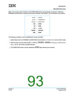
IBM SONET/SDH Framer
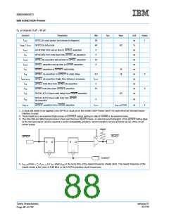
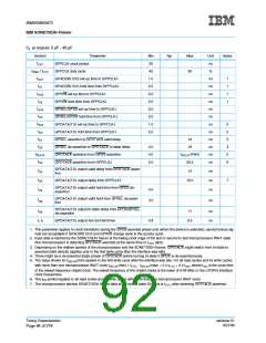
C at outputs: 5 pF - 40 pF
L
Symbol
Parameter
Min
30
Typ
Max
60
Unit
ns
%
Notes
tCYC
tPWH / tCYC
tSU1
tH1
GPPCLK clock period
GPPCLK duty cycle
40
GPADDR(13:0) set-up time to GPPCLK↓
GPADDR(13:0) hold time from GPPCLK↓
GPR/W set-up time to GPPCLK↓
1.0
2.5
6.0
2.0
6.0
2.0
1.0
2.5
ns
ns
ns
ns
ns
ns
ns
ns
ns
ns
ns
ns
1
1
1
1
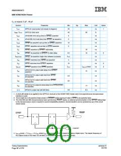
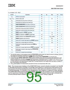
tSU2
tH2
tSU3
tH3
tSU4
tH4
GPR/W hold time from GPPCLK↓
GPSEL/GPDS set-up time to GPPCLK↓
GPSEL/GPDS hold time from GPPCLK↓
GPDATA(7:0) set-up time to GPPCLK↓
GPDATA(7:0) hold time from GPPCLK↓
GPSEL assertion to GPDTACK valid delay
GPSEL de-assertion to GPDTACK tri-state delay
GPDTACK assertion from GPDS assertion
GPDTACK assertion from GPPCLK↓
2
2
3
4
5
6
tD1
16
16
tD2
4.0
4.5
5.0
tDELAY
tD3
tDELAY(max)
20.5
15
GPDATA(7:0) output valid delay from GPDTACK asser-
tion
tD4
tD5
tH5
ns
ns
ns
GPDATA(7:0) output delay from GPPCLK↓
18.0
7
GPDATA(7:0) output valid hold time from GPDS de-
assertion
4.0
3.0
GPDATA(7:0) output valid hold from GPSEL de-asser-
tion
tH6
ns
GPDATA(7:0) output tri-state delay from GPDS/GPSEL
de-assertion
tD6
17
ns
ns
tr, tf
GPDATA(7:0) output rise and fall times
0.8
8.5
1. This parameter applies to clock transitions during the GPDS asserted phase only (when the device is selected); asynchronous sig-
nals are acceptable if GPADDR(13:0) and GPR/W change early in the access cycle.
2. Input data is latched by the SONET/SDH framer at the falling clock edge of the last or second to last microprocessor WAIT state
(the microprocessor is detecting GPDTACK asserted at the same time or tCYC later).
3. Depending on the relative speeds of the microprocessor and the SONET/SDH framer, GPDTACK might switch from tri-state to
asserted state directly (applies only to the first write cycle after the interface was idle).
4. There might be a de-asserted (high) phase of GPDTACK before turning tri-state if GPDS is de-asserted early.
5. The value shown for tDELAY(min) applies to the first write cycle after the interface was idle. For all read cycles and for write cycles
with more than one microprocessor WAIT cycle tDELAY(min) = tCYC. tDELAY(max) = 5 x tCYC + 6 x tmin, where tmin is the cycle time
of the lowest-frequency chiplet clock. The lowest frequency of the chiplet clocks is the lower of 6.48 MHz or the UTOPIA interface
clock frequencies.
6. The tD3 symbol applies to all read cycles and to write cycles with more than one microprocessor WAIT cycle.
7. The microprocessor latches SONET/SDH framer data at the end of state S4. This is tCYC after detecting GPDTACK asserted.
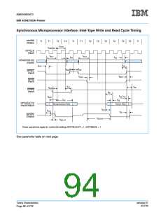
Timing Characteristics
Page 84 of 279
ssframer.01
8/27/99

 IBM [ IBM ]