IBM3009K2672
IBM SONET/SDH Framer
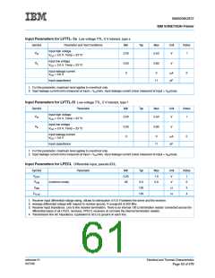
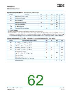
Input Parameters for PPECL Differential input, P-Pseudo-ECL
Symbol
VDIFF
VCM
Parameter
Differential input signal voltage
Common mode voltage
Min
0.3
1.8
Typ
0.6
2.0
Max
Unit
V
Notes
2.2
5
V
CIN
Input capacitance
pF
V/ns
ps
Differential input slew rate
Pulse width degradation
DC input impedance
2.0
1
160
ZRIN
100
kΩ
2
3
ZTLAC
Transmission line AC impedance
100
Ω
1. 311 MHz operation.
2. PPECL receivers do not have an internal 100 Ω termination across their inputs.
3. Equivalent to 50 Ω to ground on each line. If the common mode voltages of the attached OE module and the PPECL receiver are
compatible, a termination resistor of 100 Ω should be connected in between the negative and positive input of the receiver. If VCM
is not compatible, ‘adaptation’ can be done by shifting the supply voltage of the OE module, or by using AC coupling capacitors.
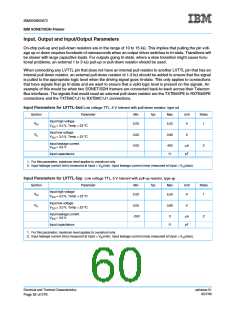
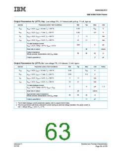
Output Parameters for LVTTL-5sd Low voltage TTL, 5 V tolerant with pull-down, 11mA, type sd
Symbol
VOH
Parameter and/or Test Conditions
VDD = 3.0 V, IOUT = 10 mA, Tj = 100 ο
Min
2.40
0.00
-7
Typ
Max
VDD
Unit
V
C
VDD = 3.0 V, IOUT = -7 mA, Tj = 100 ο
VDD = 3.0 V, VOUT = 0.4 V, Tj = 100 ο
C
VOL
IOL
0.40
V
-11
11
mA
mA
C
C
VDD = 3.0 V, VOUT = 2.4 V, Tj = 100 ο
IOH
10
Tri-state leakage current
0
400
µA
V
DD = 3.0 V, Temp = 23 οC, VOUT = VDD
Slew rate of output
Output impedance
30
45
mA/ns
Ω
35
55
11
Whole process, temperature, and VDD range
Output capacitance
pF
Electrical and Thermal Characteristics
Page 54 of 279
ssframer.01
8/27/99

 IBM [ IBM ]