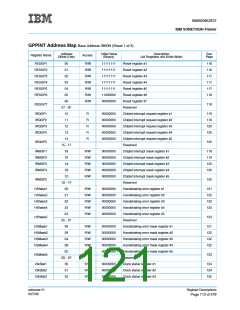
IBM3009K2672
IBM SONET/SDH Framer
select the mode of operation. When AU-4 mode is selected, an AU-4 is supplied to the SONET/SDH framer’s
transmit Telecom Bus. When AU-4 mode is selected, the AU-4 that is provided must be aligned to the TXC-
FRM pulse output and must also be frequency synchronous with either of the TXCCLK or TXCCLK clocks.
For more information on the timing modes, see Transmit Telecom Bus on page 20. In VC-4 mode, a VC-4 is
supplied to the SONET/SDH framer; the SONET/SDH framer calculates a pointer and appends it to the input
VC-4, thus creating an AU-4. When VC-4 mode is active, it is necessary to have both the C1 and J1 pulses
present in the corresponding TXTB#C1J1 signal. In 4 x STM-1/STS-3c mode, the MS and RS Overhead are
added to the AU-4 by the SONET/SDH framer and the completed frame is transmitted. In STM-4/STS-12
mode, the AU-4s are byte-interleaved, RS and MS Overhead are added to the multiplexed AU-4s, and the
completed STM-4/STS-12 frame is transmitted. When operating in 4 x STM-1/STS-3c mode or STM-4/STS-
12 mode, each transmit Telecom Bus interface can be individually configured for AU-4 or VC-4 mode.
In STM-4c/STS-12c mode, the four transmit Telecom Buses act as a single transmit Telecom Bus with a 32-
bit wide data path. The byte associated with Telecom Bus 1 is the MSB and is the first byte that is transmitted.
All of the C1J1, SPE, FAIL and clock inputs must be driven with the same signals and the GContTx#(1:0) bits
should be set to configure each macro for the same mode, either VC-4 or AU-4.
Note: POH processing is not performed when the SONET/SDH framer is operating in Telecom Bus mode.
All POH bytes in the transmit direction are derived from what is input at the transmit Telecom Bus inputs. All
POH bytes at the receive Telecom Bus interface are derived directly from the line.
Receive Telecom Bus Interface
Four output Telecom Buses are provided in the receive direction for interfacing TDM traffic from the line inter-
faces to path processing devices. Handshaking signals are provided for identifying the SPE and C1J1 bytes.
Control bits exist to configure each receive Telecom Bus interface individually as to parity generation, clock
edge selection, or C1J1 signal aligned to A23 byte only or to C1 and J1 bytes.
In STM-4/STS-12 and 4 x STM-1/STS-3c modes, the Telecom Buses act independently of each other. In
STM-4c/STS-12c modes, the four Telecom Buses act in parallel as one Telecom Bus with a 32-bit wide data
path. For details, see Receive Telecom Bus on page 23.
Microprocessor Interface
The SONET/SDH framer can support either Motorola or Intel microprocessor bus types. The Motorola inter-
face is designed to support a Motorola 68360 processor bus type interface (QUICC bus type). Either synchro-
nous or asynchronous modes of operation can be selected. In synchronous mode, all of the bus transactions
are synchronized to the microprocessor clock. In asynchronous mode, all of the bus transactions are asyn-
chronous with respect to the microprocessor clock and are synchronized internally to the external GPPCLK
signal. The Intel-compatible bus interface can also operate in a synchronous or asynchronous mode.
A watchdog timer is provided to allow transactions to a specific block to be completed when a programmable
timer runs out, even if the clock for the block being accessed is not present. If a timeout occurs, an interrupt
request bit corresponding to the offending block is set.
Boundary Scan Interface
A boundary scan interface fully compliant with IEEE Standard 1149.1-1994 (JTAG) is provided for board level
testing of the SONET/SDH framer. Details of the SONET/SDH framer boundary scan operation are provided
in the section Boundary Scan on page 262.
ssframer.01
8/27/99
Operation
Page 109 of 279

 IBM [ IBM ]