IBM3009K2672
IBM SONET/SDH Framer
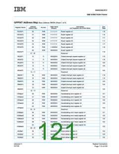
Clock Monitor Status Registers
The MAIN clock monitor status register is used as a pointer to the other clock monitor status registers with
active error indication bit(s). The clock monitor status register bits indicate the loss of a specific chiplet’s
clock. They are set whenever a difference between the clock test signal and the individual chiplets clock
acknowledge signal occurs after one clock monitor test period. To reset an individual bit of the clock monitor
status registers, the clock of the corresponding chiplet must be restored and a ‘1’ must be written into the bit
location of the register (R/W). Reading one of the registers will reset the whole (8-bit) register if the corre-
sponding “clear-register” option is set in the configuration register. All clock monitor status and pointer regis-
ters have a corresponding MASK register (R/W). Every unmasked, active clock monitor status bit causes an
active pointer bit. Every unmasked, active pointer bit causes activation of the pointer bit in the MAIN interrupt
register.
Local GPPINT Configuration Registers
There are registers (R/W) for the Clock Monitor Test Period, the Watchdog Timer Period, and the “clear-reg-
ister” option.
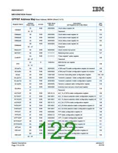
Global Static Configuration Registers
These registers contain configuration parameters that are shared by many chiplets or that are needed by
chiplets that have no GppHandler. The initial values can be modified by the microprocessor after power-on,
but should not be changed later. All global static configuration registers are R/W. In order to ensure proper
device operation the following reset procedure must be followed:
Reset Sequence:
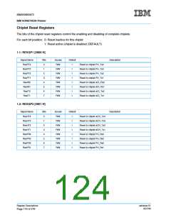
1. During power-up, the FRESET signal pin needs to be set low.
2. The FRESET signal pin can be brought high only after the GPPCLK clock has been applied.
3. After the FRESET signal is de-asserted, the microprocessor configures all of the static configuration bits
in the global GPPINT registers and sets the SIM reset bits in RESGP6-7 to ‘1’.
4. The microprocessor can selectively enable individual chiplets by deactivating the corresponding chiplet
reset bits in the RESGP1-7 registers, provided that particular chiplet’s clock is present.
5. The microprocessor then sets the configuration bits in the enabled chiplets.
6. Each chiplet also has an additional reset bit (not in the GPPINT chiplet) that must be set to ’0’ in order to
cause the chiplet to operate.
7. If it is desired to change the static configuration bits, steps 2-5 above must be performed. Changing the
register settings in an individual chiplet can be done on the fly. It should be noted that when a chiplet’s
reset bit is set to a ‘1’, the registers of that chiplet go to their default values.
Status Registers
These registers provide status information from chiplets that have no GppHandler and are read-only. Pres-
ently, there is only one status register for the SIM chiplet (PLL lock status). The bit values follow the driving
signal immediately.
Register Descriptions
Page 112 of 279
ssframer.01
8/27/99

 IBM [ IBM ]