IBM3009K2672
IBM SONET/SDH Framer
Register Descriptions
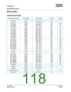
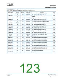
This section contains the address maps and register bit descriptions for the internal memory locations of the
SONET/SDH framer. The Access columns of the tables specify bit access as Read-only (R), Write-only (W)
or Read/Write (R/W). When writing to registers that contain bits designated in the following tables as
Reserved or Not Used, care should be taken to write those bits with their default values (if specified), or with
‘0’ if no default value is specified.
GPPINT Architecture
The General Purpose Processor interface provides direct access to registers located in the GPPINT module
and direct, but delayed, access to registers and counters located in the GppHandler modules of the various
chiplets of the SONET/SDH framer. GPPINT controls the handshaking with the external microprocessor as
well as the handshaking with the GppHandlers at the asynchronous chiplet interfaces.
Address decoding is done to the chiplet level in GPPINT. In addition, addresses are decoded to the register
level for the local GPPINT registers.
Reset Registers
Each chiplet is controlled by one reset bit. At power-on, all reset bits are active and the chiplets are disabled.
They can be released by the GPP only after all global configuration parameters have been set and the clocks
to the chiplets have been established. In addition, there are reset bits for parts of the device that do not have
their own GppHandler.
It should be noted that the bits in the GPPINT chiplet are only reset by the assertion and de-assertion of the
hardware reset pin (FRESET).
Interrupt Registers
The MAIN interrupt register is used as a pointer to the other interrupt registers with pending requests, the
MAIN clock status error register, and the MAIN handshaking error register. The interrupt bits indicate pending
interrupt requests from individual chiplets. An active bit of the interrupt registers is reset by removing the
cause for the request in the corresponding chiplet or by masking the active IRQ bit(s) in the chiplet; therefore,
the interrupt registers (including the pointer) are read-only. All interrupt and pointer registers have a corre-
sponding MASK register (R/W). Every unmasked, active interrupt bit causes an active pointer bit. Every
unmasked, active pointer bit causes activation of the interrupt signal to the microprocessor.
Handshaking Error Registers
The MAIN handshaking error register is used as a pointer to the other handshaking error registers with pend-
ing requests. Each bit of the handshaking error registers indicates a locked interface to one of the GppHan-
dlers. Two additional bits indicate various time-out events. To reset an individual bit of the handshaking error
registers, the cause for the request must be removed AND a ‘1’ must be written into the bit location of the reg-
ister (R/W). Reading one of the registers will reset the whole (8-bit) register if the corresponding “clear-regis-
ter” option is set in the configuration register. All handshaking error indication and pointer registers have a
corresponding MASK register (R/W).
Every unmasked, active handshaking error bit causes an active pointer bit. Every unmasked, active pointer
bit causes activation of the pointer bit in the MAIN interrupt register.
ssframer.01
8/27/99
Register Descriptions
Page 111 of 279

 IBM [ IBM ]