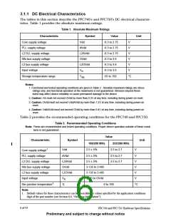
3.1.1 DC Electrical Characteristics
Th e tables in th is section describe th e PPC740’s an d PPC750’s DC electrical ch aracter-
istics. Table 1 provides th e absolu te m axim u m ratin gs.
Table 1. Absolute Maximum Ratings
Characteristic
Core supply voltage
Symbol
Value
Unit
Vdd
-0.3 to 2.75
-0.3 to 2.75
-0.3 to 2.75
-0.3 to 3.6
-0.3 to 3.6
-0.3 to 3.6
V
V
V
V
V
V
PLL supply voltage
L2 DLL supply voltage
60x bus supply voltage
L2 bus supply voltage
Input voltage
AVdd
L2AVdd
OVdd
L2OVdd
V
in
Storage temperature range
T
-55 to 150
°C
stg
Notes:
1. Functional and tested operating conditions are given in Table 2 . Absolute maximum ratings are stress
ratings only, and functional operation at the maximums is not guaranteed. Stresses beyond those
listed may affect device reliability or cause permanent damage to the device.
2. Caution: Vin must not exceed OVdd by more than 0.3V at any time, including during power-on reset.
3. Caution: OVdd must not exceed Vdd/AVdd by more than 1.2V at any time, including during power-on
reset.
4. Caution: Vdd/AVdd must not exceed OVdd by more than 0.4V at any time, including during power-on
reset.
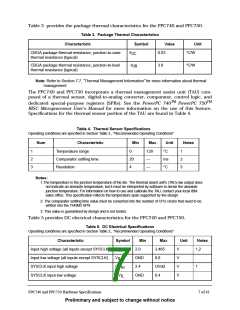
Table 2 provides th e recom m en ded operatin g con dition s for th e PPC740 an d PPC750.
Table 2. Recommended Operating Conditions
Note: These are recommended and tested operating conditions. Proper device operation outside of these condi-
tions is not guaranteed.
Value
Characteristic
Symbol
Unit
166/200 MHz
233/266 MHz
1
Vdd
2.5 ± 5%
2.5 to 2.7
V
Core supply voltage
PLL supply voltage
L2 DLL supply voltage
60x bus supply voltage
L2 bus supply voltage
Input voltage
AVdd
2.5 ± 5%
2.5 to 2.7
2.5 to 2.7
V
V
V
V
V
L2AVdd
OVdd
2.5 ± 5%
3.135 to 3.465
3.135 to 3.465
GND to OVdd
L2OVdd
V
in
1
Die-junction temperature
Tj
0 to 105
°C
Note:
1. Default values for these characteristics can be overridden by values specified by the application conditions
digit of the part number (see Section 8.0, "Ordering Information").
6 of 43
PPC740 and PPC750 Hardware Specifications
Preliminary and subject to change without notice

 IBM [ IBM ]