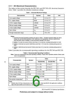
Table 5. DC Electrical Specifications (Continued)
Operating conditions are specified in Section Table 2., "Recommended Operating Conditions"
Characteristic
Symbol
Min
Max
Unit
µA
Notes
1,2
Input leakage current, V = OVdd
I
—
—
30
30
—
in
in
Hi-Z (off state) leakage current, Vin = OVdd
I
µA
V
1,2
TSI
Output high voltage, I
= –6mA
V
V
2.4
—
OH
OH
OL
Output low voltage, I
= 6 mA
0.4
5.0
V
OL
Capacitance, V =0 V, f = 1 MHz
C
—
pF
2,3
in
in
Notes:
1. For 60x bus signals, the reference is OVdd, while L2OVdd is the reference for the L2 bus signals.
2. Excludes test signals LSSD_MODE, L1_TSTCLK, L2_TSTCLK, and IEEE 1149.1 signals.
3. Capacitance values are guaranteed by design and characterization, and are not tested.
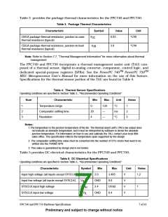
Table 6 provides th e power con su m ption for th e PPC740 an d PPC750.
Table 6. Power Consumption
Operating conditions are specified in Section Table 2., "Recommended Operating Conditions"
Processor CPU Frequency
Unit
Notes
166/200 MHz
225/233 MHz
266 MHz
Full-On Mode
Typical
4.2
5.0
5.7
7.9
W
1,3,4,5
1,2,4,5
Maximum
Doze Mode
Typical
6.0
1.6
250
100
7.0
1.8
250
100
30
W
2.1
250
100
30
W
1,2,5
1,2,5
1,2,5
1,3,5,6
Nap Mode
Typical
mW
mW
mW
Sleep Mode
Typical
Sleep Mode - PLL and DLL Disabled
Typical 30
Notes:
1. These values apply for all valid 60x bus and L2 bus ratios. The values do not include I/O Supply Power
(OVdd and L2OVdd) or PLL/DLL supply power (AVdd and L2AVdd). OVdd and L2OVdd power is sys-
tem dependent, but is typically <10% of Vdd power. Worst case power consumption for AVdd = 15 mw
and L2AVdd = 15 mW
2. Maximum power is measured at maximum Vdd specified in Section Table 2., "Recommended Operat-
ing Conditions"
3. Typical power is an average value measured at Vdd = AVdd = L2AVdd = 2.5 v (2.6 v at 233/266 MHz),
OVdd = L2OVdd = 3.3 V in a system executing typical applications and benchmark sequences.
8 of 43
PPC740 and PPC750 Hardware Specifications
Preliminary and subject to change without notice

 IBM [ IBM ]