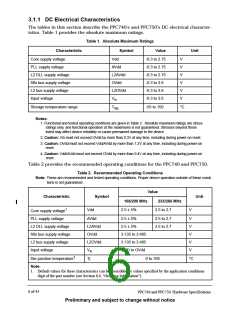
4. Full-on mode uses a worst case instruction mix.
5. Guaranteed by design and characterization, and is not tested.
6. Guaranteed and tested in Low Power Applications only, see Section 8.0, “Ordering Information“
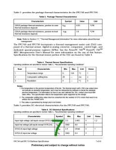
3.1.2 AC Electrical Characteristics
Th is section provides th e AC electrical ch aracteristics for th e PPC740 an d PPC750.
After fabrication , parts are sorted by m axim u m processor core frequ en cy as sh own in
Section 3.1.2.1, “Clock AC Specification s“ an d tested for con form an ce to th e AC specifi-
cation s for th at frequ en cy. Th ese specification s are for 166, 200, 225, 233, an d 266
MHz processor core frequ en cies. Th e processor core frequ en cy is determ in ed by th e
bu s (SYSCLK) frequ en cy an d th e settin gs of th e PLL_CFG(0-3) sign als. Parts are sold by
m axim u m processor core frequ en cy; see Section 1.9, "Orderin g In form ation ".
3.1.2.1 Clock AC Specifications
Table 7 provides th e clock AC tim in g specification s as defin ed in Figu re 2 .
Table 7. Clock AC Timing Specifications
Operating conditions are specified in Section Table 2., "Recommended Operating Conditions"
225/233 MHz
266 MHz
Min Max
166/200 MHz
Nu
m
Characteristic
Unit
Notes
Min
Max
Min
Max
Processor frequency
VCO frequency
150
300
25
200
400
100
40
150
300
25
233
466
100
40
150
300
25
266
533
100
40
MHz
MHz
MHz
ns
SYSCLK frequency
SYSCLK cycle time
SYSCLK rise and fall time
1
1
12
12
12
2,3
4
—
2.0
60
—
2.0
60
—
2.0
60
ns
2,3
3
SYSCLK duty cycle mea-
sured at 1.4 V
40
40
40
%
SYSCLK jitter
—
—
±150
—
—
±150
—
—
±150 ps
100 µs
4,3
5
Internal PLL relock time
100
100
Notes:
1. Caution: The SYSCLK frequency and the PLL_CFG[0-3] settings must be chosen such that the result-
ing SYSCLK (bus) frequency, CPU (core) frequency, and PLL (VCO) frequency do not exceed their
respective maximum or minimum operating frequencies. Refer to the PLL_CFG[0-3] signal description
in Section 7.1, “PLL Configuration“ for valid PLL_CFG[0-3] settings.
2. Rise and fall times for the SYSCLK input are measured from 0.4 to 2.4 V.
3. Timing is guaranteed by design and characterization, and is not tested.
4. The total input jitter (short term and long term combined) must be under ±150 ps.
5. Relock timing is guaranteed by design and characterization, and is not tested. PLL-relock time is the
maximum amount of time required for PLL lock after a stable Vdd and SYSCLK are reached during
the power-on reset sequence. This specification also applies when the PLL has been disabled and
subsequently re-enabled during sleep mode. Also note that HRESET must be held asserted for a min-
imum of 255 bus clocks after the PLL-relock time during the power-on reset sequence.
*
Subject to availability - see your marketing representative.
PPC740 and PPC750 Hardware Specifications
9 of 43
Preliminary and subject to change without notice

 IBM [ IBM ]