IBM PowerPC 403GCX
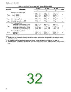
Symbol
Table 19. 403GCX DRAM Interface Timing Relationships
25 MHz
33 MHz
40 MHz
Units
Parameter
Min
Min
Min
Available CAS Access Time:
2-1-1-1 access
3-2-2-2 access
0.5T -2.5
0.5T -2.5
0.5T -2.5
C
C
C
ns
T
CAS
1.5T -2.5
1.5T -2.5
1.5T -2.5
C
C
C
0.5T -2.5
0.5T -2.5
0.5T -2.5
3-1-1-1 access
C
C
C
0.5T -2.5
0.5T -2.5
0.5T -2.5
ns
ns
CAS Precharge Time
T
C
C
C
CP
0.5T -4.0
0.5T -4.0
0.5T -4.0
Write Data Setup Time to CAS
T
C
C
C
DS
RAS Precharge Time:
1.5T -2.5
1.5T -2.5
1.5T -2.5
BRn[ERM] = 0 and BRn[PCC] = 0
BRn[ERM] = 0 and BRn[PCC] = 1
BRn[ERM] = 1 and BRn[PCC] = 0
BRn[ERM] = 1 and BRn[PCC] = 1
C
C
C
2.5T -2.5
2.5T -2.5
2.5T -2.5
ns
ns
T
C
C
C
RP
1.25T -1.0
1.25T -1.0
1.25T -1.0
C
C
C
2.25T -1.0
2.25T -1.0
2.25T -1.0
C
C
C
RAS Active During Refresh:
BR[RAR] = 0
1.5T -1.5
1.5T -1.5
1.5T -1.5
T
C
C
C
RAS
2.5T -1.5
2.5T -1.5
2.5T -1.5
BR[RAR] = 1
C
C
C
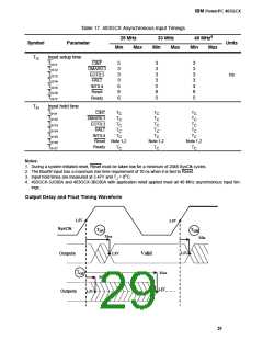
Note:
1. Relationships are guaranteed by design and are not tested. Relationships also assume 50 pF capacitive loading
on interface signals.
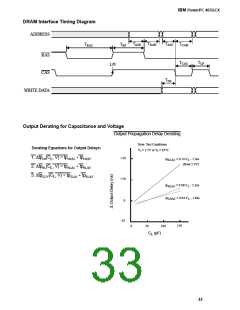
2. For detailed DRAM interface timing waveforms, refer to "DRAM Interface Timing Diagram," on page 33.
3. 403GCX-3JC80A and 403GCX-3BC80A with application relief applied meet all 40 MHz interface timing relation-
ships.
32

 IBM [ IBM ]