APCPCWM_4828539:WP_0000001WP_0000001
1
H27(U_S)4G8_6F2D
4 Gbit (512M x 8 bit) NAND Flash
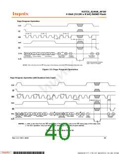
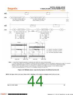
Page Program Operation
CLE
CE
tWC
tWC
tWC
WE
ALE
RE
tADL
tWB
tPROG
tWHR
Coꢄꢈ
Add±
Roꢆꢈ
Add3
Coꢄꢈ
Add1
Roꢆꢈ
Add±
Roꢆꢈ
Add1
Din
N
Din
M
I/Ox
R/B
82ꢇ
12ꢇ
72ꢇ
I/O2
Seriaꢄ Data
Input Command
Proꢅram
Command
Read Status
Command
1 up to m Bꢂte
Seriaꢄ Input
Coꢄumn Address
Roꢆ Address
I/O2=2 Successꢁuꢄ Proꢅram
I/O2=1 Error in Proꢅram
NOTES: tADL is tꢇe time ꢁrom tꢇe WE risinꢅ edꢅe oꢁ ꢁinaꢄ address cꢂcꢄe to tꢇe WE risinꢅ edꢅe oꢁ ꢁirst data cꢂcꢄeꢈ
Figure 15: Page Program Operation
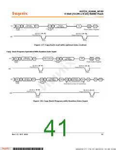
Page Program Operation with Random Data Input
CLE
CE
tWC
tWC
tWC
WE
tADL
tADL
tWHR
tWB
tPROG
ALE
RE
Col.
Add1
Col.
Add2
Col.
Add1
Col.
Add2
Row
Add1
Row
Add2
Row
Add3
Din
Din
J
Din
N
Din
K
85h
IOx
R/B
12ꢇ
80h
70h
IO0
M
Read Status
Command
Serial Data
Input Command
Random Data
Proꢅram
Command
Column Address
Column Address
Column Address
Serial Input
Input Command
NOTES : 1. tADL is the time from the WE risinig edge of final address cycle to the WE rising edge of first data cycle.
2. For EDC operation. only one time random data input is possible at same address.
Figure 16: Random Data In
Rev 1.4 / OCT. 2010
40
B34416/177.179.157.84/2010-10-08 10:08
*ba53f20d-240c*

 HYNIX [ HYNIX SEMICONDUCTOR ]