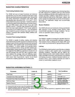
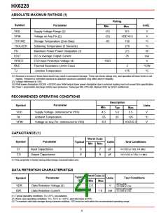
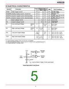
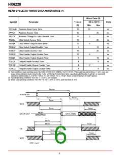
HX6228
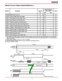
WRITE CYCLE AC TIMING CHARACTERISTICS (1)
Worst Case (3)
-55 to 125°C
Symbol
Parameter
Typical
(2)
Units
Min
Max
TAVAVW Write Cycle Time (4)
13
9
25
20
20
15
20
0
ns
ns
ns
ns
ns
ns
ns
ns
ns
ns
ns
ns
TWLWH Write Enable Write Pulse Width
TSLWH
TDVWH
TAVWH
TWHDX
TAVWL
TWHAX
TWLQZ
Chip Select to End of Write Time
12
9
Data Valid to End of Write Time
Address Valid to End of Write Time
Data Hold Time after End of Write Time
Address Valid Setup to Start of Write Time
Address Valid Hold after End of Write Time
Write Enable to Output Disable Time
10
0
0
0
0
0
5
0
9
TWHQX Write Disable to Output Enable Time
TWHWL Write Recovery Time
12
4
5
5
TEHWH
Chip Enable to End of Write Time
11
20
(1) Test conditions: input switching levels VIL/VIH=0.5V/VDD-0.5V (CMOS), VIL/VIH=0V/3V (TTL), input rise and fall times <1 ns/V, input and
output timing reference levels shown in the Tester AC Timing Characteristics table, capacitive output loading >50 pF, or equivalent capacitive
load of 5 pF for TWLQZ.
(2) Typical operating conditions: VDD=5.0 V, TA=25°C, pre-radiation.
(3) Worst case operating conditions: VDD=4.5 V to 5.5 V, -55 to 125°C, post total dose at 25°C.
(4) TAVAVW = TWLWH + TWHWL.
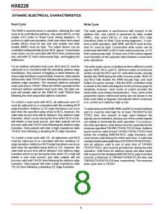
T
AVAVW
ADDRESS
T
AVWH
TWHAX
T
AVWL
T
WHWL
TWLWH
NWE
T
WLQZ
T
WHQX
DATA OUT
DATA IN
HIGH
IMPEDANCE
T
DVWH
TWHDX
DATA VALID
T
SLWH
NCS
CE
T
EHWH
7

 HONEYWELL [ Honeywell ]