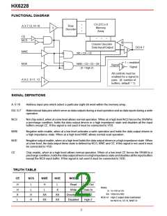
HX6228
RADIATION CHARACTERISTICS
Total Ionizing Radiation Dose
The SRAM will meet any functional or electrical specifica-
tion after exposure to a radiation pulse up to the transient
dosesurvivabilityspecification,whenappliedunderrecom-
mended operating conditions. Note that the current con-
ducted during the pulse by the RAM inputs, outputs, and
power supply may significantly exceed the normal operat-
ing levels. The application design must accommodate
these effects.
The SRAM will meet all stated functional and electrical
specifications over the entire operating temperature range
afterthespecifiedtotalionizingradiationdose. Allelectrical
and timing performance parameters will remain within
specifications after rebound at VDD = 5.5 V and T =125°C
extrapolatedtotenyearsofoperation. Totaldosehardness
isassuredbywaferleveltestingofprocessmonitortransis-
tors and RAM product using 10 KeV X-ray and Co60
radiation sources. Transistor gate threshold shift correla-
tions have been made between 10 KeV X-rays applied at
a dose rate of 1x10⁵ rad(SiO2)/min at T = 25°C and gamma
rays (Cobalt 60 source) to ensure that wafer level X-ray
testing is consistent with standard military radiation test
environments.
Neutron Radiation
The SRAM will meet any functional or timing specification
after exposure to the specified neutron fluence under
recommended operating or storage conditions. This as-
sumes an equivalent neutron energy of 1 MeV.
Soft Error Rate
Transient Pulse Ionizing Radiation
The SRAM is capable of meeting the specified Soft Error
Rate (SER), under recommended operating conditions.
This hardness level is defined by the Adams 90% worst
case cosmic ray environment for geosynchronous orbits.
The SRAM is capable of writing, reading, and retaining
storeddataduringandafterexposuretoatransientionizing
radiation pulse up to the specified transient dost rate upset
specification, when applied under recommended operat-
ing conditions. To ensure validity of all specified perfor-
mance parameters before, during, and after radiation (tim-
ing degradation during transient pulse radiation is ≤20%),
it is suggested that stiffening capacitance be placed on or
near the package VDD and VSS, with a maximum induc-
tance between the package (chip) and stiffening capaci-
tance of 0.7 nH per part. If there are no operate-through or
valid stored data requirements, typical circuit board
mounted de-coupling capacitors are recommended.
Latchup
TheSRAMwillnotlatchupduetoanyoftheaboveradiation
exposure conditions when applied under recommended
operating conditions. Fabrication with the SIMOX sub-
strate material provides oxide isolation between adjacent
PMOS and NMOS transistors and eliminates any potential
SCR latchup structures. Sufficient transistor body tie con-
nections to the p- and n-channel substrates are made to
ensure no source/drain snapback occurs.
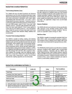
RADIATION HARDNESS RATINGS (1)
Test Conditions
Limits (2)
Units
Parameter
Total Dose
≥1x10⁶
≥1x10¹¹
≥1x10¹²
<1x10⁻¹⁰
≥1x10¹⁴
rad(SiO2)
rad(Si)/s
TA=25°C
Pulse width ≤1 µs
Transient Dose Rate Upset (3)
Transient Dose Rate Survivability
Soft Error Rate
Pulse width ≤50 ns, X-ray,
VDD=6.0 V, TA=25°C
rad(Si)/s
TA=125°C, Adams 90%
upsets/bit-day
N/cm2
worst case environment
1 MeV equivalent energy,
Unbiased, TA=25°C
Neutron Fluence
(1) Device will not latch up due to any of the specified radiation exposure conditions.
(2) Operating conditions (unless otherwise specified): VDD=4.5 V to 5.5 V, -55°C to 125°C.
(3) Applies to 40-lead flat pack only. Assume ≥1x1009 rad(Si))/s for 32-lead flat pack. Stiffening capacitance is suggested for optimum expected
dose rate upset performance as stated above.
3

 HONEYWELL [ Honeywell ]