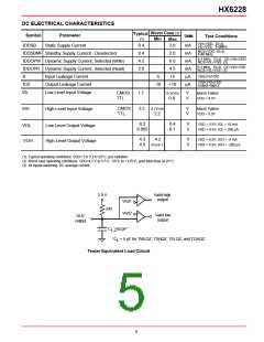
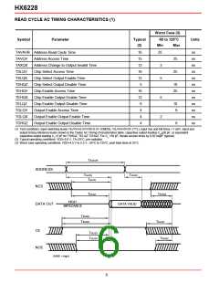
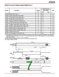
HX6228
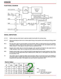
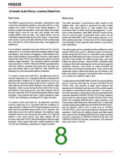
FUNCTIONAL DIAGRAM
131,072 x 8
Memory
Array
•
•
•
A:3-7,12,14-16
Row
Decoder
9
CE
•
•
•
NCS
8
Column Decoder
Data Input/Output
DQ:0-7
8
NWE
NOE
WE • CS • CE
1 = enabled
Signal
NWE • CS • CE • OE
(0 = high Z)
Signal
#
All controls must be
enabled for a signal to
pass. (#: number of
buffers, default = 1)
A:0-2, 8-11, 13
8
SIGNAL DEFINITIONS
A: 0-16
DQ: 0-7
Address input pins which select a particular eight-bit word within the memory array.
Bidirectional data pins which serve as data outputs during a read operation and as data inputs during a write
operation.
NCS
Not chip select, when at a low level allows normal operation. When at a high level NCS forces the SRAM to
a precharge condition, holds the data output drivers in a high impedance state and disables all the input
buffers except CE. If this signal is not used it must be connected to VSS.
NWE
NOE
Negative write enable, when at a low level activates a write operation and holds the data output drivers in
a high impedance state. When at a high level NWE allows normal read operation.
Negative output enable, when at a high level holds the data output drivers in a high impedance state. When
at a low level, the data output driver state is defined by NCS, NWE and CE. If this signal is not used it must
be connected to VSS.
CE
Chip enable, when at a high level allows normal operation. When at a low level CE forces the SRAM to a
prechargecondition, holdsthedataoutputdriversinahighimpedancestateanddisablesalltheinputbuffers
except the NCS input buffer. If this signal is not used it must be connected to VDD.
TRUTH TABLE
CE
NCS
NWE
NOE
MODE
DQ
H
H
X
L
L
L
H
L
L
Read
Write
Data Out
Data In
Notes:
X
X: VI=VIH or VIL
XX: VSS≤VI≤VDD
NOE=H: High Z output state maintained
for NCS=X, CE=X, NWE=X
H
X
XX
XX
XX
XX
Deselected High Z
Disabled High Z
2

 HONEYWELL [ Honeywell ]