HT46R01A
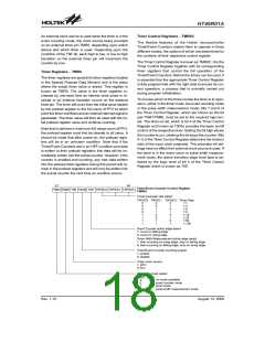
turns to its original low level. As before, the T0ON bit will
be automatically reset to zero and the timer will stop
counting. It is important to note that in the Pulse Width
Measurement Mode, the T0ON bit is automatically reset
to zero when the external control signal on the external
timer pin returns to its original level, whereas in the other
two modes the T0ON bit can only be reset to zero under
program control. The residual value in the timer, which
can now be read by the program, therefore represents
the length of the pulse received on the external timer
pin. As the T0ON bit has now been reset, any further
transitions on the external timer pin, will be ignored. Not
until the T0ON bit is again set high by the program can
the timer begin further pulse width measurements. In
this way, single shot pulse measurements can be easily
made. It should be noted that in this mode the counter is
controlled by logical transitions on the external timer pin
and not by the logic level. As in the case of the other two
modes, when the counter is full, the timer will overflow
and generate an internal interrupt signal. The counter
will also be reset to the value already loaded into the
preload register. If the external timer pin is pin-shared
with other I/O pins, to ensure that the pin is configured to
operate as a pulse width measuring input pin, two things
have to happen. The first is to ensure that the
T0M1/T0M0 bits place the Timer/Event Counter in the
pulse width measuring mode, the second is to ensure
that the port control register configures the pin as an in-
put. It should be noted that a timer overflow and corre-
sponding timer interrupt is one of the wake-up sources.
Note that the timer interrupts can be disabled by ensur-
ing that the ET0I bits in the INTC0 register are reset to
zero.
counter, driven by the system clock and if applicable, di-
vided by the prescaler value, will begin to count-up from
this preloaded register value until full, at which point an
overflow signal will be generated, causing the PFD out-
put to change state. The counter will then be automati-
cally reloaded with the preload register value and once
again continue counting-up.
For the PFD output to function, it is essential that the
corresponding bit of the Port A control register PAC bit 1
is setup as an output. If setup as an input the PFD output
will not function, however, the pin can still be used as a
normal input pin. The PFD output will only be activated if
bit PA1 is set to ²1². This output data bit is used as the
on/off control bit for the PFD output. Note that the PFD
output will be low if the PA1 output data bit is cleared to
²0².
Using this method of frequency generation, and if a
crystal oscillator is used for the system clock, very pre-
cise values of frequency can be generated.
Prescaler
Bits T0PSC0~T0PSC2 of the TMR0C register can be
used to define a division ratio for the internal clock
source of the Timer/Event Counter enabling longer time
out periods to be setup.
I/O Interfacing
The Timer/Event Counter, when configured to run in the
event counter or pulse width measurement mode, re-
quires the use of the external timer pin for its operation.
As this pin is a shared pin it must be configured correctly
to ensure that it is setup for use as a Timer/Event Coun-
ter input pin. This is achieved by ensuring that the mode
select bits in the Timer/Event Counter control register,
select either the event counter or pulse width measure-
ment mode. Additionally the corresponding PAC Port
Control Register bit must be set high to ensure that the
pin is setup as an input. Any pull-high resistor connected
to this pin will remain valid even if the pin is used as a
Timer/Event Counter input.
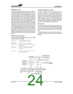
Programmable Frequency Divider - PFD
The PFD output is pin-shared with the I/O pin PA1. The
PFD on/off function and its timer source are selected via
bits in the CTRL0 register, however, if not selected, the
pin can operate as a normal I/O pin. The timer overflow
signal is the clock source for the PFD circuit. The output
frequency is controlled by loading the required values
into the timer register and if available the timer prescaler
registers to give the required frequency. The timer/event
T
i
m
e
r
O
v
e
r
f
l
o
w
P
F
D
C
l
o
c
k
P
A
1
D
a
t
a
P
F
D
O
u
t
p
u
t
a
t
P
A
1
PFD Output Control
Rev. 1.10
20
August 13, 2008

 HOLTIC [ HOLT INTEGRATED CIRCUITS ]