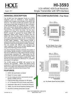
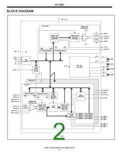
HI-3593
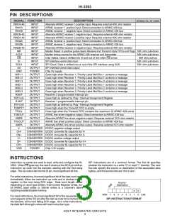
PIN DESCRIPTIONS
SIGNAL FUNCTION
DESCRIPTION
INTERNAL PULL UP / DOWN
RIN1A-40
RIN1A
RIN1B
RIN1B-40
RIN2A-40
RIN2A
RIN2B
RIN2B-40
MR
INPUT
INPUT
Alternate ARINC receiver 1 positive input. Requires external 40K ohm resistor
ARINC receiver 1 positive input. Direct connection to ARINC 429 bus
ARINC receiver 1 negative input. Direct connection to ARINC 429 bus
Alternate ARINC receiver 1 negative input. Requires external 40K ohm resistor
Alternate ARINC receiver 2 positive input. Requires external 40K ohm resistor
ARINC receiver 2 positive input. Direct connection to ARINC 429 bus
ARINC receiver 2 negative input. Direct connection to ARINC 429 bus
Alternate ARINC receiver 2 negative input. Requires external 40K ohm resistor
INPUT
INPUT
INPUT
INPUT
INPUT
INPUT
INPUT
Master Reset. A positive pulse clears Receive and Transmit data FIFOs and flags 50K ohm pull-down
ACLK
CS
INPUT
Master timing source for the ARINC 429 receiver and transmitter
Chip Select. Data is shifted into SI and out of SO when CS is low.
SPI interface serial data input
50K ohm pull-down
50K ohm pull-up
INPUT
SI
INPUT
50K ohm pull-down
50K ohm pull-down
SCLK
SO
INPUT
SPI Clock. Data is shifted into or out of the SPI interface using SCK
SPI interface serial data output
OUTPUT
POWER
OUTPUT
OUTPUT
OUTPUT
OUTPUT
OUTPUT
OUTPUT
OUTPUT
OUTPUT
OUTPUT
OUTPUT
OUTPUT
OUTPUT
OUTPUT
OUTPUT
OUTPUT
OUTPUT
GND
Chip 0V supply
MB1-1
MB1-2
MB1-3
MB2-1
MB2-2
MB2-3
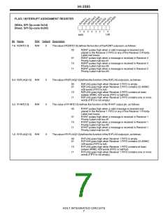
R2INT
R2FLAG
R1INT
R1FLAG
TEMPTY
TFULL
TXBOUT
AMPB
TXAOUT
AMPA
V-
Goes high when Receiver 1, Priority-Label Mail Box 1 contains a message
Goes high when Receiver 1, Priority-Label Mail Box 2 contains a message
Goes high when Receiver 1, Priority-Label Mail Box 3 contains a message
Goes high when Receiver 2, Priority-Label Mail Box 1 contains a message
Goes high when Receiver 2, Priority-Label Mail Box 2 contains a message
Goes high when Receiver 2, Priority-Label Mail Box 3 contains a message
Receiver 2 programmable Interrupt pin
Goes high as defined by Flag / Interrupt Assignment Register
Receiver 1 programmable Interrupt pin
Goes high as defined by Flag / Interrupt Assignment Register
Goes high when the Transmit FIFO is empty
Goes high when the Transmit FIFO contains the maximum 32 ARINC 429 words
ARINC line driver negative output. Direct connection to ARINC 429 bus
Alternate ARINC line driver negative output. Requires external 32.5 ohm resistor
ARINC line driver positive output. Direct connection to ARINC 429 bus
Alternate ARINC line driver positive output. Requires external 32.5 ohm resistor
CONVERTER DC/DC negative voltage output
CONVERTER DC/DC converter fly capacitor for V-
CONVERTER DC/DC converter fly capacitor for V-
CONVERTER DC/DC positive voltage output
CONVERTER DC/DC converter fly capacitor for V+
CONVERTER DC/DC converter fly capacitor for V+
CN-
CN+
V+
CP-
CP+
VDD
POWER
Chip 3.3V supply
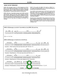
INSTRUCTIONS
Instruction op codes are used to read, write and configure the HI-
3593. When CS goes low, the next 8 clocks at the SCK pin shift an
instruction op code into the decoder, starting with the first rising
edge. The op code is fed into the SI pin, most significant bit first.
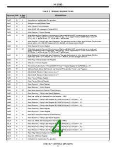
SPI Instructions are of a common format. The first bit specifies
whether the instruction is a write “0” or read “1” transfer. The next
five bits specify the source or destination of the associated data
byte(s), and the last two bits are “don’t care”.
For write instructions, the most significant bit of the data word must
immediately follow the instruction op code and is clocked into its
register on the next rising SCK edge. Data word length varies
depending on word type written: 8-bit Control Register writes, 32-
bit ARINC label writes or 256-bit writes to a channel’s label-
matching enable/disable memory.
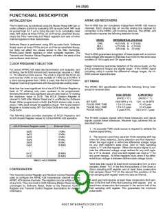
Source /
Destination
X
1
X
0
MSB
7
6
5
4
3
2
LSB
For read instructions, the most significant bit of the requested data
word appears at the SO pin after the last op code bit is clocked into
the decoder, at the next falling SCK edge. As in write instructions,
the data field bit-length varies with read instruction type.
SPI INSTRUCTION FORMAT
HOLT INTEGRATED CIRCUITS
3

 HOLTIC [ HOLT INTEGRATED CIRCUITS ]