HT95LXXX
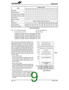
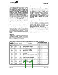
Stack Register
The special function registers are located from 00H to
1FH. The embedded control registers are located in the
memory areas from 20H to 3FH. The remaining spaces
which are not specified in the following table before the
40H are reserved for future expanded usage and read-
ing these locations will get ²00H². The general purpose
data memory is divided into 15 banks (HT95L400/40P),
11 banks (HT95L300/30P), 6 banks (HT95L200/20P,
HT95L100/10P) or 2 banks (HT95L000/00P). The
banks in the RAM are all addressed from 40H to 0FFH
and they are selected by setting the value of the bank
pointer (BP).
This is a special part of the memory which is used to
save the contents of the program counter only. The
stack is organized into 12 levels (HT95L400/40P), 8 lev-
els (HT95L300/30P, HT95L200/20P, HT95L100/10P) or
4 levels (HT95L000/00P) and is neither part of the data
nor part of the program space, and is neither readable
nor writable. The activated level is indexed by the stack
pointer (SP) and is neither readable nor writable. At a
subroutine call or interrupt acknowledge signal, the con-
tents of the program counter are pushed onto the stack.
At the end of a subroutine or an interrupt routine, sig-
naled by a return instruction (RET or RETI), the program
counter is restored to its previous value from the stack.
After a chip reset, the SP will point to the top of the stack.
If the stack is full and an interrupt takes place, the inter-
rupt request flag will be recorded but the acknowledge
signal will be inhibited even if this interrupt is enabled.
When the stack pointer is decremented (by RET or
RETI), the interrupt will be serviced. This feature pre-
vents stack overflow allowing the programmer to use the
structure more easily. If the stack is full and a ²CALL² is
subsequently executed, stack overflow occurs and the
first entry will be lost (only the most recent 12, 8 or 4, de-
pending on various MCU type, returned addresses are
stored).
All of the data memory areas can handle arithmetic,
logic, increment, decrement and rotate operations di-
rectly. Except for some dedicated bits, each bit in the
data memory can be set and reset by ²SET [m].i² and
²CLR [m].i². They are also indirectly accessible through
memory pointer registers (MP0 or MP1). The
bank1~bank14 and bank27 are only indirectly accessi-
ble through memory pointer 1 register (MP1).
The LCD display memory is located at bank 1BH. They
can be read and written to by the indirect addressing
mode using memory pointer 1 (MP1). To turn the display
On or Off, a ²1² or ²0² is written to the corresponding bit
of the memory area.
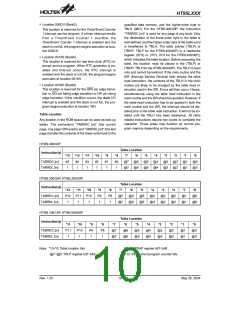
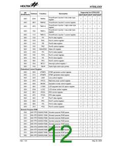
Data Memory
The data memory is divided into four functional groups:
special function registers, embedded control register,
LCD display memory and general purpose memory.
Most are read/write, but some are read only.
Special Register, Embedded Control Register, LCD Display Memory and General Purpose RAM
Supported for HT95LXXX
400/P 300/P 200/P 100/P 000/P
BP
(RAM Bank)
Address
Function
Description
Special Function Register
00H
00H
00H
00H
00H
00H
00H
00H
00H
00H
00H
00H
00H
01H
02H
03H
04H
05H
06H
07H
08H
09H
0AH
0BH
IAR0
MP0
Indirect addressing register 0
Memory pointer register 0
Indirect addressing register 1
Memory pointer register 1
Bank Pointer register
Ö
Ö
Ö
Ö
Ö
Ö
Ö
Ö
Ö
Ö
Ö
Ö
Ö
Ö
Ö
Ö
Ö
Ö
Ö
Ö
Ö
Ö
Ö
Ö
Ö
Ö
Ö
Ö
Ö
Ö
Ö
Ö
Ö
Ö
Ö
Ö
Ö
Ö
Ö
Ö
Ö
Ö
Ö
Ö
Ö
Ö
Ö
Ö
Ö
Ö
Ö
Ö
Ö
Ö
Ö
Ö
Ö
Ö
Ö
Ö
IAR1
MP1
BP
ACC
Accumulator
PCL
Program counter lower-order byte register
Table pointer
TBLP
TBLH
WDTS
STATUS
INTC0
Table higher-order byte register
Watchdog Timer option setting register
Status register
Interrupt control register 0
Timer/Event Counter 0 high-order byte
register
00H
0CH
TMR0H
Ö
Ö
Ö
Ö
Ö
Rev. 1.20
11
May 26, 2004

 HOLTEK [ HOLTEK SEMICONDUCTOR INC ]