Preliminary
HT48R06A-1
next instruction execution, this will be executed
immediately after the dummy period is fin-
ished.
V
D
D
R
E
S
t
S
S
T
S
S
T
T
i
m
e
-
o
u
t
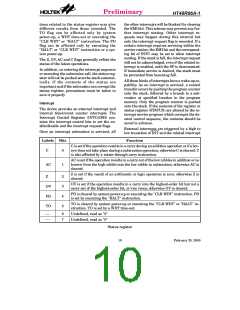
To minimize power consumption, all the I/O
pins should be carefully managed before enter-
ing the HALT status.
C
h
i
p
R
e
s
e
t
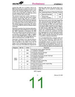
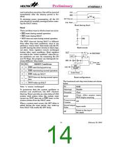
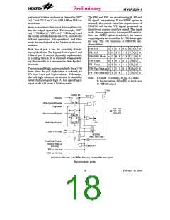
Reset timing chart
Reset
V
D
D
There are three ways in which a reset can occur:
·
·
·
RES reset during normal operation
RES reset during HALT
WDT time-out reset during normal operation
R
E
S
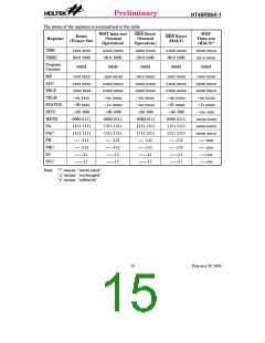
The WDT time-out during HALT is different
from other chip reset conditions, since it can
perform a "warm reset" that resets only the PC
and SP, leaving the other circuits in their origi-
nal state. Some registers remain unchanged
during other reset conditions. Most registers
are reset to the ²initial condition² when the re-
set conditions are met. By examining the PD
and TO flags, the program can distinguish be-
tween different "chip resets".
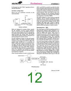
Reset circuit
H
A
L
T
W
a
r
m
R
e
s
e
t
W
D
T
R
E
S
C
R
o
e
l
s
d
TO PD
RESET Conditions
RES reset during power-up
RES reset during normal operation
RES wake-up HALT
e
t
S
S
T
1
1
0
-
b
i
t
R
i
p
p
l
e
O
S
C
0
u
0
0
u
1
C
o
u
n
t
e
r
S
y
s
t
e
m
R
e
s
e
t
WDT time-out during normal opera-
tion
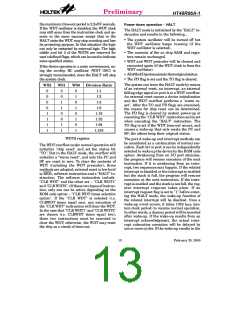
Reset configuration
1
1
u
1
The functional unit chip reset status are shown
below.
WDT wake-up HALT
PC
000H
Note: "u" means "unchanged"
Interrupt
Prescaler
Disable
Clear
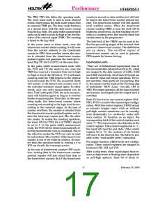
To guarantee that the system oscillator is
started and stabilized, the SST (System
Start-up Timer) provides an extra-delay of 1024
system clock pulses when the system reset
(power-up, WDT time-out or RES reset) or the
system awakes from the HALT state.
Clear. After master reset,
WDT begins counting
WDT
Timer/event
Counter
Off
When a system reset occurs, the SST delay is
added during the reset period. Any wake-up
from HALT will enable the SST delay.
Input/output
Ports
Input mode
Points to the top of
the stack
SP
14
February 25, 2000

 HOLTEK [ HOLTEK SEMICONDUCTOR INC ]