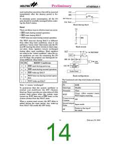
Preliminary
HT48R06A-1
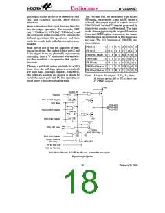
put/output latches can be set or cleared by "SET
[m].i" and "CLR [m].i" (m=12H, 14H or 16H) in-
structions.
The PB0 and PB1 are pin-shared with BZ and
BZ signal, respectively. If the BZ/BZ option is
selected, the output signal in output mode of
PB0/PB1 will be the PFD signal generated by
timer/event counter overflow signal. The input
mode always remaining its original functions.
Once the BZ/BZ option is selected, the buzzer
output signals are controlled by PB0 data regis-
ter only. The I/O functions of PB0/PB1 are
shown below.
Some instructions first input data and then fol-
low the output operations. For example, "SET
[m].i", "CLR [m].i", "CPL [m]", "CPLA [m]" read
the entire port states into the CPU, execute the
defined operations (bit-operation), and then
write the results back to the latches or the accu-
mulator.
PB0 I/O
PB1 I/O
I
I
I
I
I
O O O O O O
I O O O
Each line of port A has the capability of wak-
ing-up the device. The highest 6-bit of port C and
5 bits of port B are not physically implemented;
on reading them a "0" is returned whereas writ-
ing then results in a no-operation. See Applica-
tion note.
O O O
I
I
PB0/PB1 Mode x C B B C B B C B B
PB0 Data
PB1 Data
x
x
0
1 D 0 1 D0
0
x
1
x
x D x
x
I
x x x D1
There is a pull-high option available for all I/O
lines. Once the pull-high option is selected, all
I/O lines have pull-high resistors. Otherwise,
the pull-high resistors are absent. It should be
noted that a non-pull-high I/O line operating in
input mode will cause a floating state.
PB0 Pad Status I
I
I
D 0 B D0 0 B
I D1 0 B
PB1 Pad Status I D 0 B
I
I
Note: I: input; O: output; D, D0, D1: data;
B: buzzer option, BZ or BZ; x: don't care
C: CMOS output
V
D
D
C
o
n
t
r
o
l
B
U
i
t
P
D
a
t
a
B
u
s
D
C
Q
K
Q
B
R e
W
r
i
t
e
C
o
n
t
r
e
o
l
g
i
s
t
e
r
S
t
C
h
i
p
R
s
e
P
P
P
A
B
C
0
0
~
~
P
P
A
B
7
2
0
~
P
C
1
R
e
a
d
C
o
n
t
r
o
l
R
e
g
i
s
t
e
r
D
a
t
a
B
i
t
D
C
Q
K
Q
B
g
W
r
i
t
e
D
a
t
a
R
e
i
s
t
e
r
S
M
U
P
B
0
(
P
B
0
,
P
B
1
O
n
l
y
)
X
E
X
T
E
X
T
E
N
M
(
P
B
0
,
P
B
1
O
n
l
y
)
U
X
R
e
a
d
D
a
t
a
R
e
g
i
s
t
e
r
S
y
s
t
e
m
W
a
k
e
-
u
p
O
P
0
~
O
P
7
(
P
A
o
n
l
y
)
I
N
T
f
o
r
P
C
0
O
n
l
y
T
M
R
f
o
r
P
C
1
O
n
l
y
E
X
T
=
B
Z
f
o
r
P
B
0
o
n
l
y
,
E
X
T
=
B
Z
f
o
r
P
B
1
o
n
l
y
,
c
o
n
t
r
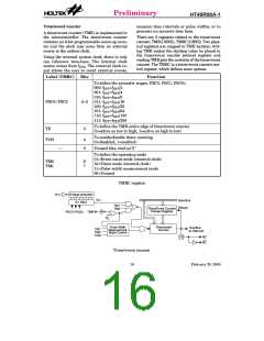
Input/output ports
18
February 25, 2000

 HOLTEK [ HOLTEK SEMICONDUCTOR INC ]