HT46R064G/065G/0662G
Enhanced A/D Type 8-Bit OTP MCU with OPA
Pulse Width Modulator
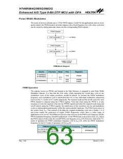
The series of devices includes up to 2 8-bit PWM outputs. Useful for the applications such as motor
speed control, the PWM function provides outputs with a fixed frequency but with a duty cycle that
can be varied by setting particular values into the corresponding PWM register.
P
W
M
0
R
e
g
i
s
t
e
r
8
-
b
i
t
C
o
m
p
a
r
P
a
M
t
o
W
r
0
0
P
W
M
1
R
e
g
i
s
t
e
r
8
-
b
i
t
C
o
m
p
a
r
P
a
M
t
o
W
r
1
1
8
-
b
i
t
/
(
7
+
1
)
/
(
6
+
2
)
P
W
M
C
o
u
n
t
e
r
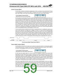
PWM Block Diagram
Device
Channels Mode
Pins
Registers
HT46R064G
HT46R065G
1
PA4
PWM0
6+2
7+1
PD0
PD1
PWM0
PWM1
HT46R0662G
2
PWM Operation
The register, known as PWMn and located in the Data Memory, is assigned to each Pulse Width
Modulator channel. It is here that the 8-bit value, which represents the overall duty cycle of one
modulation cycle of the output waveform, should be placed. To increase the PWM modulation
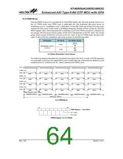
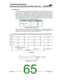
frequency, each modulation cycle is subdivided into two or four individual modulation subsections,
known as the 7+1 mode or 6+2 mode respectively. The required mode and the on/off control for each
PWM channel is selected using the CTRL0 register. Note that when using the PWM, it is only
necessary to write the required value into the PWMn register and select the required mode setup and
on/off control using the CTRL0 register, the subdivision of the waveform into its sub-modulation
cycles is implemented automatically within the microcontroller hardware. The PWM clock source is
the system clock fSYS. This method of dividing the original modulation cycle into a further 2 or 4
sub-cycles enable the generation of higher PWM frequencies which allow a wider range of
applications to be served. The difference between what is known as the PWM cycle frequency and the
PWM modulation frequency should be understood. As the PWM clock is the system clock, fSYS, and as
the PWM value is 8-bits wide, the overall PWM cycle frequency is fSYS/256. However, when in the 7+1
mode of operation the PWM modulation frequency will be fSYS/128, while the PWM modulation
frequency for the 6+2 mode of operation will be fSYS/64.
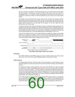
PWM Modulation
PWM Cycle Frequency
PWM Cycle Duty
fSYS/64 for (6+2) bits mode
fSYS/256
[PWM]/256
f
SYS/128for (7+1) bits mode
Rev. 1.00
63
March 3, 2011

 HOLTEK [ HOLTEK SEMICONDUCTOR INC ]