HT46R064G/065G/0662G
Enhanced A/D Type 8-Bit OTP MCU with OPA
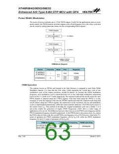
PWM Output Control
The PWM outputs are pin-shared with the I/O pins PA4, PD0 and PD3 respectively depending upon
the selected device. To operate as a PWM output and not as an I/O pin, the correct bits must be set in
the CTRL0 register. A zero value must also be written to the corresponding I/O Port Control bit to
ensure that the corresponding PWM output pin is setup as an output. After these two initial steps have
been carried out, and of course after the required PWM value has been written into the PWMn register,
writing a high value to the corresponding I/O Output Data bit will enable the PWM data to appear on
the pin. Writing a zero value will disable the PWM output function and force the output low. In this
way, the Port data output registers can be used as an on/off control for the PWM function. Note that if
the CTRL0 register has selected the PWM function, but a high value has been written to its
corresponding I/O Port Control bit to configure the pin as an input, then the pin can still function as a
normal input line, with pull-high resistor options.
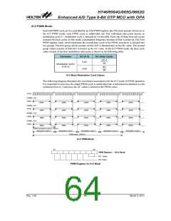
PWM Programming Example
The following sample program shows how the PWM0 output is setup and controlled.
mov
mov
set
set
clr
set
:
a,64h
pwm0,a
ctrl0.5
ctrl0.3
pac.7
pa.7
; setup PWM value of decimal 100
; select the 7+1 PWM mode
; select pin PA7 to have a PWM function
; setup pin PA7 as an output
; enable the PWM output
:
pa.7
clr
; disable the PWM output_ pin
; PA7 forced low
Rev. 1.00
66
March 3, 2011

 HOLTEK [ HOLTEK SEMICONDUCTOR INC ]