HT46R064G/065G/0662G
Enhanced A/D Type 8-Bit OTP MCU with OPA
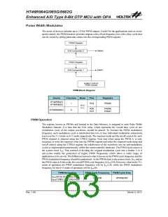
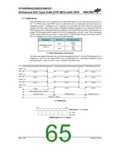
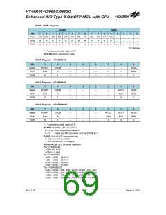
7+1 PWM Mode
Each full PWM cycle, as it is controlled by an 8-bit PWM register, has 256 clock periods. However, in
the 7+1 PWM mode, each PWM cycle is subdivided into two individual sub-cycles known as
modulation cycle 0 ~ modulation cycle 1, denoted as i in the table. Each one of these two sub-cycles
contains 128 clock cycles. In this mode, a modulation frequency increase of two is achieved. The 8-bit
PWM register value, which represents the overall duty cycle of the PWM waveform, is divided into two
groups. The first group which consists of bit1~bit7 is denoted here as the DC value. The second group
which consists of bit0 is known as the AC value. In the 7+1 PWM mode, the duty cycle value of each of
the two modulation sub-cycles is shown in the following table.
Parameter
AC (0~1)
DC (Duty Cycle)
DC+1
128
i<AC
Modulation cycle i
(i=0~1)
DC
i³AC
128
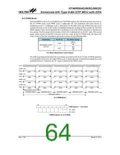
7+1 Mode Modulation Cycle Values
The following diagram illustrates the waveforms associated with the 7+1 mode PWM operation. It is
important to note how the single PWM cycle is subdivided into 2 individual modulation cycles,
numbered 0 and 1 and how the AC value is related to the PWM value.
f
S
Y
S
[
[
[
[
P
P
P
P
W
W
W
W
M
M
M
M
]
]
]
]
=
=
=
=
1
1
1
1
0
0
0
0
0
1
2
3
P
P
P
P
W
W
W
W
M
M
M
M
5
5
5
0
1
1
/
/
/
1
1
1
2
2
2
8
8
8
5
5
5
5
0
0
1
1
/
/
/
/
1
1
1
1
2
2
2
2
8
8
8
8
5
5
5
5
0
1
1
2
/
/
/
/
1
1
1
1
2
2
2
2
8
8
8
8
5
2
/
1
2
8
P
W
M
m
o
d
u
l
a
S
t
Y
i
S
o
n
p
e
r
i
o
d
:
1
2
8
/
f
M
o
d
u
l
a
t
i
o
n
c
y
c
l
e
0
M
o
d
u
l
a
t
i
o
n
c
y
c
l
e
M
o
1
d
u
l
a
t
i
o
P
W
M
c
y
S
c
Y
l
S
e
:
2
5
6
/
f
7+1 PWM Mode
b
7
b
0
P
W
M
R
e
g
i
s
t
e
r
(
7
A
D
C
v
a
l
u
u
e
C
v
a
l
e
PWM Register for 7+1 Mode
Rev. 1.00
65
March 3, 2011

 HOLTEK [ HOLTEK SEMICONDUCTOR INC ]