HT46R64/HT46C64
LCD Display Memory
C
O
M
4
0
H
4
1
H
4
2
H
4
3
H
5
E
H
5
F
H
6
0
H
B
i
t
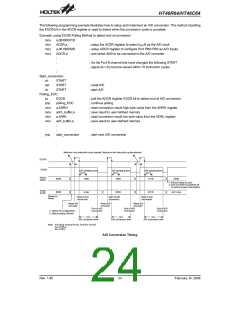
The device provides an area of embedded data memory
for LCD display. This area is located from 40H to 60H of
the RAM at Bank 1. Bank pointer (BP; located at 04H of
the RAM) is the switch between the RAM and the LCD
display memory. When the BP is set as ²1², any data
written into 40H~60H will effect the LCD display. When
the BP is cleared to ²0² or ²1², any data written into
40H~60H means to access the general purpose data
memory. The LCD display memory can be read and writ-
ten to only by indirect addressing mode using MP1.
When data is written into the display data area, it is auto-
matically read by the LCD driver which then generates
the corresponding LCD driving signals. To turn the dis-
play on or off, a ²1² or a ²0² is written to the correspond-
ing bit of the display memory, respectively. The figure
illustrates the mapping between the display memory
and LCD pattern for the device.
0
1
2
3
0
1
2
3
S
E
G
M
E
N
T
0
1
2
3
3
0
3
1
3
2
Display Memory
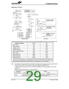
duty). The bias type LCD driver can be ²R² type or ²C²
type. If the ²R² bias type is selected, no external capaci-
tor is required. If the ²C² bias type is selected, a capaci-
tor mounted between C1 and C2 pins is needed. The
LCD driver bias voltage can be 1/2 bias or 1/3 bias by
option. If 1/2 bias is selected, a capacitor mounted be-
tween V2 pin and ground is required. If 1/3 bias is se-
lected, two capacitors are needed for V1 and V2 pins.
Refer to application diagram.
LCD Driver Output
The output number of the device LCD driver can be 33´2
or 33´3 or 32´4 by option (i.e., 1/2 duty, 1/3 duty or 1/4
V
V
A
B
V
V
V
C
S
A
C
O
M
0
S
S
S
S
S
V
V
B
C
C
O
M
1
V
V
S
A
V
V
B
C
C
O
M
2
V
V
S
A
V
V
B
C
C
O
M
3
V
V
S
A
V
B
V
V
C
S
L
C
C
D
s
e
g
m
e
n
t
s
O
N
O
M
2
s
i
d
e
l
i
g
h
t
e
d
N
o
t
e
:
1
/
4
d
u
t
y
,
1
/
3
b
i
a
s
,
C
t
y
p
e
:
"
V
A
"
3
/
2
V
L
C
D
,
"
V
B
"
V
L
C
D
,
"
V
C
"
1
/
2
V
L
C
D
1
/
4
d
u
t
y
,
1
/
3
b
i
a
s
,
R
t
y
p
e
:
"
V
A
"
V
L
C
D
,
"
V
B
"
2
/
3
V
L
C
D
,
"
V
C
"
1
/
3
V
L
C
D
LCD Driver Output
Rev. 1.80
25
February 14, 2006
图片预览")
 HOLTEK [ HOLTEK SEMICONDUCTOR INC ]