HT46R64/HT46C64
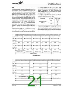
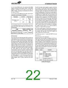
In a (7+1) bits PWM function, the contents of the PWM
register is divided into two groups. Group 1 of the PWM
register is denoted by DC which is the value of
PWM.7~PWM.1. The group 2 is denoted by AC which is
the value of PWM.0.
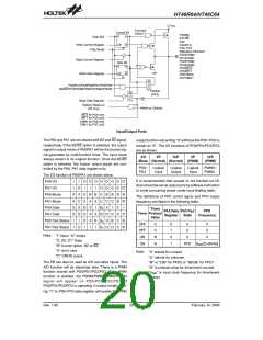
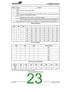
The A/D converter control register is used to control the
A/D converter. The bit2~bit0 of the ADCR are used to
select an analog input channel. There are a total of eight
channels to select. The bit5~bit3 of the ADCR are used
to set PB configurations. PB can be an analog input or
as digital I/O line decided by these 3 bits. Once a PB line
is selected as an analog input, the I/O functions and
pull-high resistor of this I/O line are disabled and the A/D
converter circuit is powered-on. The EOCB bit (bit6 of
the ADCR) is end of A/D conversion flag. Check this bit
to know when A/D conversion is completed. The START
bit of the ADCR is used to begin the conversion of the
A/D converter. Giving START bit a rising edge and fall-
ing edge means that the A/D conversion has started. In
order to ensure that the A/D conversion is completed,
the START should remain at ²0² until the EOCB is
cleared to ²0² (end of A/D conversion).
In a (7+1) bits mode PWM cycle, the duty cycle of each
modulation cycle is shown in the table.
Parameter
AC (0~1)
Duty Cycle
DC+1
128
i<AC
Modulation cycle i
(i=0~1)
DC
i³AC
128
The modulation frequency, cycle frequency and cycle
duty of the PWM output signal are summarized in the
following table.
Bit 7 of the ACSR register is used for test purposes only
and must not be used for other purposes by the applica-
tion program. Bit1 and bit0 of the ACSR register are
used to select the A/D clock source.
PWM
PWM Cycle PWM Cycle
Modulation Frequency Frequency
Duty
f
f
SYS/64 for (6+2) bits mode
f
SYS/256
[PWM]/256
SYS/128 for (7+1) bits mode
The EOCB bit is set to ²1² when the START bit is set
from ²0² to ²1².
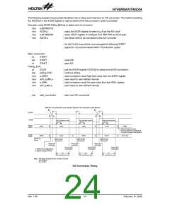
A/D Converter
Important Note for A/D initialization:
The 8 channels and 10 bits resolution A/D converter are
implemented in this microcontroller. The reference volt-
age is VDD. The A/D converter contains 4 special regis-
ters which are; ADRL (24H), ADRH (25H), ADCR (26H)
and ACSR (27H). The ADRH and ADRL are A/D result
register higher-order byte and lower-order byte and are
read-only. After the A/D conversion is completed, the
ADRH and ADRL should be read to get the conversion
result data. The ADCR is an A/D converter control regis-
ter, which defines the A/D channel number, analog
channel select, start A/D conversion control bit and the
end of A/D conversion flag. If the users want to start an
A/D conversion, define PB configuration, select the con-
verted analog channel, and give START bit a rising edge
and falling edge (0®1®0). At the end of A/D conver-
sion, the EOCB bit is cleared. The ACSR is A/D clock
setting register, which is used to select the A/D clock
source.
Special care must be taken to initialize the A/D con-
verter each time the Port B A/D channel selection bits
are modified, otherwise the EOCB flag may be in an un-
defined condition. An A/D initialization is implemented
by setting the START bit high and then clearing it to zero
within 10 instruction cycles of the Port B channel selec-
tion bits being modified. Note that if the Port B channel
selection bits are all cleared to zero then an A/D initial-
ization is not required.
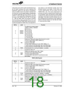
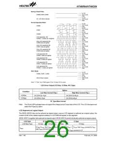
Bit No. Label
Function
Selects the A/D converter clock
source
0
1
ADCS0 00= system clock/2
01= system clock/8
10= system clock/32
11= undefined
ADCS1
2~6
7
¾
Unused bit, read as ²0²
TEST For test mode used only
ACSR (27H) Register
Rev. 1.80
22
February 14, 2006
图片预览")
 HOLTEK [ HOLTEK SEMICONDUCTOR INC ]