HT46R64/HT46C64
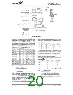
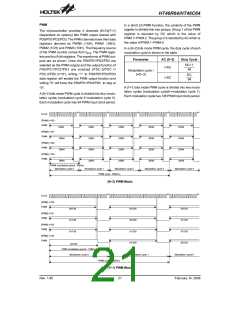
PWM
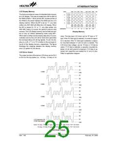
In a (6+2) bit PWM function, the contents of the PWM
register is divided into two groups. Group 1 of the PWM
register is denoted by DC which is the value of
PWM.7~PWM.2. The group 2 is denoted by AC which is
the value of PWM.1~PWM.0.
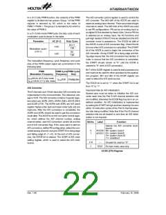
The microcontroller provides 4 channels (6+2)/(7+1)
(dependent on options) bits PWM output shared with
PD0/PD1/PD2/PD3. The PWM channels have their data
registers denoted as PWM0 (1AH), PWM1 (1BH),
PWM2 (1CH) and PWM3 (1DH). The frequency source
of the PWM counter comes from fSYS. The PWM regis-
ters are four 8-bit registers. The waveforms of PWM out-
puts are as shown. Once the PD0/PD1/PD2/PD3 are
selected as the PWM outputs and the output function of
PD0/PD1/PD2/PD3 are enabled (PDC.0/PDC.1/
PDC.2/PDC.3=²0²), writing ²1² to PD0/PD1/PD2/PD3
data register will enable the PWM output function and
writing ²0² will force the PD0/PD1/PD2/PD3 to stay at
²0².
In a (6+2) bits mode PWM cycle, the duty cycle of each
modulation cycle is shown in the table.
Parameter
AC (0~3)
Duty Cycle
DC+1
64
i<AC
Modulation cycle i
(i=0~3)
DC
64
i³AC
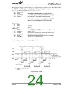
A (7+1) bits mode PWM cycle is divided into two modu-
lation cycles (modulation cycle0~modulation cycle 1).
Each modulation cycle has 128 PWM input clock period.
A (6+2) bits mode PWM cycle is divided into four modu-
lation cycles (modulation cycle 0~modulation cycle 3).
Each modulation cycle has 64 PWM input clock period.
S
Y
S
[
[
[
[
P
P
P
P
W
W
W
W
M
M
M
M
]
]
]
]
=
=
=
=
1
1
1
1
0
0
0
0
0
1
2
3
P
P
P
P
W
W
W
W
M
M
M
M
2
5
/
6
4
2
2
2
2
5
5
6
6
/
/
/
/
6
6
6
6
4
4
4
4
2
2
2
2
5
5
5
6
/
/
/
/
6
6
6
6
4
4
4
4
2
2
2
2
5
5
5
5
/
/
/
/
6
6
6
6
4
4
4
4
2
2
2
2
5
6
6
6
/
/
/
/
6
6
6
6
4
4
4
4
2
6
/
6
4
2
6
/
6
4
2
6
/
6
4
P
W
M
m
o
d
u
l
a
t
i
o
n
p
e
r
i
o
d
:
6
4
/
f
M
o
d
u
l
a
t
i
o
n
c
y
c
l
e
0
M
o
d
u
l
a
t
i
o
n
c
y
c
l
e
1
M
o
d
u
l
a
t
i
o
n
c
y
c
l
e
2
M
o
d
u
l
a
t
i
o
n
c
y
c
l
e
3
M
o
d
u
l
a
t
i
o
n
c
y
c
l
e
0
P
W
M
c
y
c
l
e
:
2
5
6
/
f
(6+2) PWM Mode
S
Y
S
[
P
W
M
]
=
1
0
0
P
W
M
5
5
5
0
1
1
/
/
/
1
1
1
2
2
2
8
8
8
5
0
/
1
2
8
5
0
/
1
2
8
[
[
[
P
P
P
W
W
W
M
M
M
]
]
]
=
=
=
1
1
1
0
0
0
1
2
3
P
P
P
W
W
W
M
M
M
5
0
/
1
2
8
5
1
/
1
2
8
5
1
/
1
2
8
5
1
/
1
2
8
5
1
/
1
2
8
5
2
/
1
2
8
5
2
/
1
2
8
P
W
M
m
o
d
u
l
a
t
i
o
n
p
e
r
i
o
d
:
1
2
8
/
f
M
o
d
u
l
a
t
i
o
n
c
y
c
l
e
0
M
o
d
u
l
a
t
i
o
n
c
y
c
l
e
1
M
o
d
u
l
a
t
i
o
n
c
y
c
l
e
0
P
W
M
c
y
c
l
e
:
2
5
6
/
f
(7+1) PWM Mode
Rev. 1.80
21
February 14, 2006
图片预览")
 HOLTEK [ HOLTEK SEMICONDUCTOR INC ]