HT46R64/HT46C64
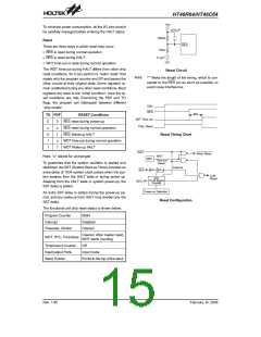
To enable the counting operation, the Timer ON bit
(T0ON: bit 4 of TMR0C; T1ON: bit 4 of TMR1C) should
be set to 1. In the pulse width measurement mode, the
T0ON/T1ON is automatically cleared after the measure-
ment cycle is completed. But in the other two modes, the
T0ON/T1ON can only be reset by instructions. The
overflow of the Timer/Event Counter 0/1 is one of the
wake-up sources and can also be applied to a PFD (Pro-
grammable Frequency Divider) output at PA3 by op-
tions. Only one PFD (PFD0 or PFD1) can be applied to
PA3 by options. If PA3 is set as PFD output, there are
two types of selections; One is PFD0 as the PFD output,
the other is PFD1 as the PFD output. PFD0, PFD1 are
the timer overflow signals of the Timer/Event Counter 0,
Timer/Event Counter 1 respectively. No matter what the
operation mode is, writing a 0 to ET0I or ET1I disables
the related interrupt service. When the PFD function is
selected, executing ²SET [PA].3² instruction to enable
PFD output and executing ²CLR [PA].3² instruction to
disable PFD output.
or 18H). For output operation, all the data is latched and
remains unchanged until the output latch is rewritten.
Each I/O line has its own control register (PAC, PBC,
PDC) to control the input/output configuration. With this
control register, CMOS output or Schmitt Trigger input
with or without pull-high resistor structures can be re-
configured dynamically under software control. To func-
tion as an input, the corresponding latch of the control
register must write ²1². The input source also depends
on the control register. If the control register bit is ²1²,
the input will read the pad state. If the control register bit
is ²0², the contents of the latches will move to the inter-
nal bus. The latter is possible in the ²read-modify-write²
instruction.
For output function, CMOS is the only configuration.
These control registers are mapped to locations 13H,
15H and 19H.
After a chip reset, these input/output lines remain at high
levels or floating state (depending on pull-high options).
Each bit of these input/output latches can be set or
cleared by ²SET [m].i² and ²CLR [m].i² (m=12H, 14H or
18H) instructions.
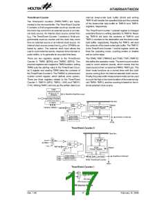
In the case of timer/event counter OFF condition, writing
data to the timer/event counter preload register also re-
loads that data to the timer/event counter. But if the
timer/event counter is turn on, data written to the
timer/event counter is kept only in the timer/event coun-
ter preload register. The timer/event counter still contin-
ues its operation until an overflow occurs.
Some instructions first input data and then follow the
output operations. For example, ²SET [m].i², ²CLR
[m].i², ²CPL [m]², ²CPLA [m]² read the entire port states
into the CPU, execute the defined operations
(bit-operation), and then write the results back to the
latches or the accumulator.
When the timer/event counter (reading TMR0/TMR1) is
read, the clock is blocked to avoid errors, as this may re-
sults in a counting error. Blocking of the clock should be
taken into account by the programmer. It is strongly rec-
ommended to load a desired value into the TMR0/TMR1
register first, before turning on the related timer/event
counter, for proper operation since the initial value of
TMR0/TMR1 is unknown. Due to the timer/event coun-
ter scheme, the programmer should pay special atten-
tion on the instruction to enable then disable the timer
for the first time, whenever there is a need to use the
timer/event counter function, to avoid unpredictable re-
sult. After this procedure, the timer/event function can
be operated normally.
Each line of port A has the capability of waking-up the
device.
Each I/O port has a pull-high option. Once the pull-high
option is selected, the I/O port has a pull-high resistor,
otherwise, there¢s none. Take note that a non-pull-high
I/O port operating in input mode will cause a floating
state.
The PA3 is pin-shared with the PFD signal. If the PFD
option is selected, the output signal in output mode of
PA3 will be the PFD signal generated by timer/event
counter overflow signal. The input mode always retain
its original functions. Once the PFD option is selected,
the PFD output signal is controlled by PA3 data register
only. Writing ²1² to PA3 data register will enable the PFD
output function and writing 0 will force the PA3 to remain
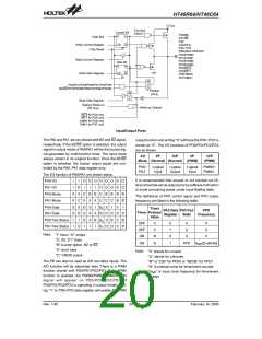
at ²0². The I/O functions of PA3 are shown below.
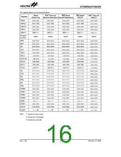
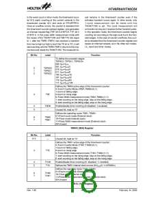
The bit0~bit2 of the TMR0C can be used to define the
pre-scaling stages of the internal clock sources of
timer/event counter 0. The definitions are as shown. The
overflow signal of timer/event counter can be used to
generate the PFD signal. The timer prescaler is also
used as the PWM counter.
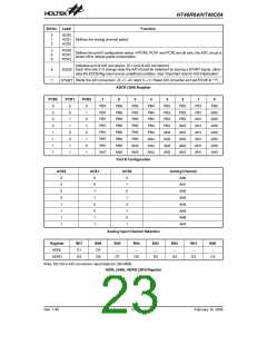
I/O
I/P
O/P
I/P
O/P
Mode (Normal) (Normal)
(PFD)
(PFD)
Input/Output Ports
Logical
Input
Logical
Output
Logical
Input
PFD
There are 24 bidirectional input/output lines in the
microcontroller, labeled as PA, PB and PD, which are
mapped to the data memory of [12H], [14H] and [18H]
respectively. All of these I/O ports can be used for input
and output operations. For input operation, these ports
are non-latching, that is, the inputs must be ready at the
T2 rising edge of instruction ²MOV A,[m]² (m=12H, 14H
PA3
(Timer on)
Note: The PFD frequency is the timer/event counter
overflowfrequencydividedby2.
The PA0, PA1, PA3, PD4, PD5, PD6 and PD7 are
pin-shared with BZ, BZ, PFD, INT0, INT1, TMR0 and
TMR1 pins respectively.
Rev. 1.80
19
February 14, 2006
图片预览")
 HOLTEK [ HOLTEK SEMICONDUCTOR INC ]