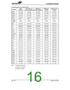
HT46R64/HT46C64
V
D
D
P
u
l
l
-
h
i
g
h
C
o
n
t
r
o
l
B
i
t
O
p
t
i
o
n
P
A
0
/
/
B
B
Z
Z
D
Q
D
a
t
a
B
u
s
P
A
1
P
A
2
W
r
i
t
e
C
o
n
t
r
o
l
R
e
g
i
s
t
e
r
C
K
P
A
3
4
0
/
~
/
P
A
F
N
D
Q
P
A
P
A
7
S
C
h
i
p
R
e
s
e
t
P
B
0
~
P
B
7
/
A
N
7
P
D
0
/
P
W
W
W
W
M
0
1
2
3
P
D
1
/
P
M
R
e
a
d
C
o
n
t
r
o
l
R
e
g
i
s
t
e
r
P
D
2
/
P
M
D
a
t
a
B
i
t
P
D
3
/
P
M
D
C
Q
P
D
4
/
I
N
T
0
1
P
D
5
/
I
N
T
K
Q
W
r
i
t
e
D
a
t
a
R
e
g
i
s
t
e
r
P
P
D
D
6
7
/
/
T
T
M
M
R
0
S
R
1
M
U
P
A
0
/
P
A
1
/
P
A
3
/
P
D
0
/
P
D
1
/
P
D
2
/
P
D
3
X
B
Z
/
B
Z
/
P
F
D
/
P
W
M
0
/
P
W
M
1
/
P
W
M
2
/
P
W
M
3
P
F
D
E
N
M
(
P
A
3
)
U
X
R
e
a
d
D
a
t
a
R
e
g
i
s
t
e
r
S
y
s
t
e
m
W
a
k
e
-
u
p
W
a
k
e
-
u
p
O
p
t
i
o
n
s
(
P
A
o
n
l
y
)
I
N
T
T
0
f
o
r
P
D
4
o
n
l
y
I
N
1
f
o
r
P
D
5
o
n
l
y
T
M
R
0
f
f
o
o
r
r
P
P
D
6
o
o
n
n
l
l
y
y
T
M
R
1
D
7
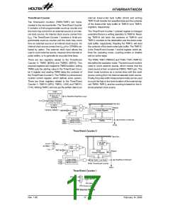
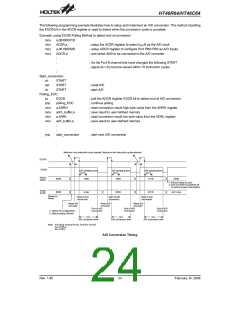
Input/Output Ports
The PA0 and PA1 are pin-shared with BZ and BZ signal,
respectively. If the BZ/BZ option is selected, the output
signal in output mode of PA0/PA1 will be the buzzer sig-
nal generated by multi-function timer. The input mode
always remain in its original function. Once the BZ/BZ
option is selected, the buzzer output signal are con-
trolled by the PA0, PA1 data register only.
output function and writing ²0² will force the PD0~PD3 to
remain at ²0². The I/O functions of PD0/PD1/PD2/PD3
are as shown.
I/O
I/P
O/P
I/P
O/P
Mode (Normal) (Normal) (PWM)
(PWM)
PD0~
PD3
Logical
Input
Logical
Output
Logical
Input
PWM0~
PWM3
The I/O function of PA0/PA1 are shown below.
It is recommended that unused or not bonded out I/O
lines should be set as output pins by software instruction
to avoid consuming power under input floating state.
PA0 I/O
I
I
I
O
I
O
I
O
I
O
O
O
O
B
C
0
O
O
B
C
1
O
O
B
B
0
O
O
B
B
1
PA1 I/O
O
X
C
X
D
I
PA0 Mode
PA1 Mode
PA0 Data
X
X
X
X
I
C
X
D
X
D
I
B
X
0
X
0
I
B
X
1
C
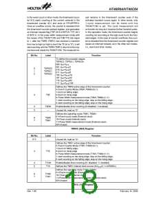
The definitions of PFD control signal and PFD output
frequency are listed in the following table.
C
D0
Timer
PA3 Data PA3 Pad
PFD
Timer Preload
Value
PA1 Data
X D1 D
D
B
D
X
0
X
B
B
Register
State
Frequency
PA0 Pad Status
PA1 Pad Status
B
I
D0
D1
0
OFF
OFF
ON
X
X
N
N
0
1
0
1
0
U
X
I
D
D
0
X
Note:
²I² input; ²O² output
²D, D0, D1² Data
0
X
ON
PFD
f
TMR/[2´(M-N)]
²B² buzzer option, BZ or BZ
²X² don¢t care
Note:
²X² stands for unused
²U² stands for unknown
²C² CMOS output
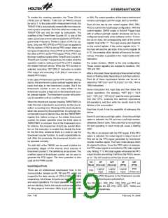
The PB can also be used as A/D converter inputs. The
A/D function will be described later. There is a PWM
function shared with PD0/PD1/PD2/PD3. If the PWM
function is enabled, the PWM0/PWM1/PWM2/PWM3
signal will appear on PD0/PD1/PD2/PD3 (if
PD0/PD1/PD2/PD3 is operating in output mode). Writ-
ing ²1² to PD0~PD3 data register will enable the PWM
²M² is ²256² for PFD0 or ²65536² for PFD1
²N² is preload value for timer/event counter
²fTMR² is input clock frequency for timer/event
counter
Rev. 1.80
20
February 14, 2006
图片预览")
 HOLTEK [ HOLTEK SEMICONDUCTOR INC ]