HT46R23/HT46C23
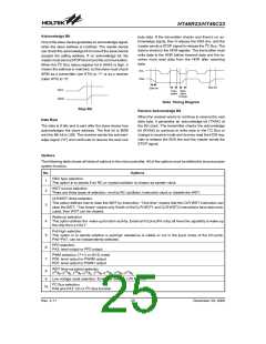
Acknowledge Bit
byte data. If the transmitter checks and there¢s no ac-
knowledge signal, then it release the SDA line, and the
master sends a STOP signal to release the I2C Bus. The
data is stored in the HDR register. The transmitter must
write data to the HDR before transmit data and the re-
ceiver must read data from the HDR after receiving
data.
One of the slave device generates an acknowledge signal,
when the slave address is matched. The master device
can check this acknowledge bit to know if the slave device
accepts the calling address. If no acknowledge bit, the
master must send a STOP bit and end the communication.
When the I2C Bus status register bit 6 HAAS is high, it
means the address is matched, so the slave must check
SRW as a transmitter (set HTX) to ²1² or as a receiver
(clear HTX) to ²0².
S
C
L
S
D
A
S
t
o
p
b
i
t
S
t
a
r
t
b
i
t
S
C
L
D
a
t
a
D
a
t
a
s
t
a
b
l
e
a
l
l
o
w
c
h
a
n
g
e
S
D
A
Data Timing Diagram
Receive Acknowledge Bit
Stop Bit
When the receiver wants to continue to receive the next
data byte, it generates an acknowledge bit (TXAK) at
the 9th clock. The transmitter checks the acknowledge
bit (RXAK) to continue to write data to the I2C Bus or
change to receive mode and dummy read the HDR reg-
ister to release the SDA line and the master sends the
STOP signal.
Data Byte
The data is 8 bits and is sent after the slave device has
acknowledges the slave address. The first bit is MSB
and the 8th bit is LSB. The receiver sends the acknowl-
edge signal (²0²) and continues to receive the next one
Options
The following table shows all kinds of options in the microcontroller. All of the options must be defined to ensure proper
system function.
No.
Options
OSC type selection.
1
This option is to decide if an RC or crystal oscillator is chosen as system clock.
WDT source selection.
2
3
There are three types of selection: on-chip RC oscillator, instruction clock or disable the WDT.
CLRWDT times selection.
This option defines how to clear the WDT by instruction. ²One time² means that the CLR WDT instruction can
clear the WDT. ²Two times² means only if both of the CLR WDT1 and CLR WDT2 instructions have been exe-
cuted, then WDT can be cleared.
Wake-up selection.
4
This option defines the wake-up function activity. External I/O pins (PA only) all have the capability to wake-up
the chip from a HALT.
Pull-high selection.
5
6
7
This option is to decide whether a pull-high resistance is visible or not in the input mode of the I/O ports.
PA0~PA7, can be independently selected.
PFD selection.
PA3: level output or PFD output
PWM selection: (7+1) or (6+2) mode
PD0: level output or PWM0 output
PD1: level output or PWM1 output
WDT time-out period selection.
212/fS~213/fS, 213/fS~214/fS, 214/fS~215/fS, 215/fS~216/fS.
8
9
Low voltage reset selection: Enable or disable LVR function.
I2C Bus selection.
PA6 and PA7: I/O or I2C Bus function
10
Rev. 2.11
25
December 29, 2008
图片预览")
 HOLTEK [ HOLTEK SEMICONDUCTOR INC ]