HT46RU25/HT46CU25
·
·
·
Location 014H
Data Memory - RAM
This area is reserved for the I2C Bus interrupt service
program. If the I2C Bus interrupt resulting from a slave
address is matched or has completed one byte of data
transfer, and if the interrupt is enabled and the stack is
not full, the program begins execution at location
014H.
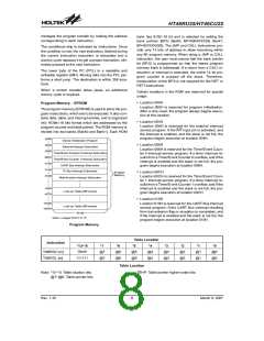
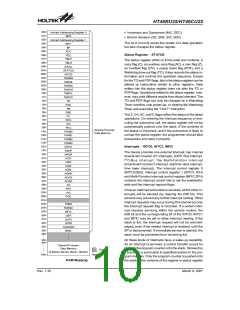
The data memory (RAM) has a structure of 628´8 bits,
and is divided into two functional groups, namely; spe-
cial function registers (52´8 bits) and general purpose
data memory (576´8 bits) most of which are read-
able/writeable, although some are read only. The gen-
eral purpose data memory is divided into three banks
(Bank0~Bank2), each bank contains 192´8 bits. Bank0
can be read from and written to by directly addressing or
indirectly addressing mode using MP0, Bank1 and
Bank2 can be read from and written to only by indirect
addressing mode using MP1. The special function reg-
isters are overlapped in all banks.
Location 018H
This area is reserved for the Multi-function interrupt
service program. If a timer interrupt results from a
Timer/Event Counter 2 overflow, or a real time clock
time-out, or Time base time-out, and if the interrupt is
enable and the stack is not full, the program begins
execution at location 018H.
Table location
The unused space before 40H is reserved for future ex-
pansion use and reading these locations returns the re-
sult ²00H². The space before 40H is overlapping in each
bank. The general purpose data memory, addressed
from 40H to FFH (Bank0; BP=0 , Bank1; BP=1 or
Bank2; BP=2), is used for data and control information
under instruction commands. All of the data memory ar-
eas can handle arithmetic, logic, increment, decrement
and rotate operations directly. Except for some dedi-
cated bits, each bit in the data memory can be set and
reset by ²SET [m].i² and ²CLR [m].i². They are also indi-
rectly accessible through memory pointer registers
(MP0;01H/MP1;03H). The space before 40H is overlap-
ping in each bank.
Any location in the ROM can be used as a look-up ta-
ble. The instructions ²TABRDC [m]² (page specified
by TBHP) and ²TABRDL [m]² (the last page) transfer
the contents of the lower-order byte to the specified
data memory, and the contents of the higher-order
byte to TBLH (Table Higher-order byte register) (08H).
Only the destination of the lower-order byte in the ta-
ble is well-defined; the other bits of the table word are
all transferred to the lower portion of TBLH. The TBLH
is read only, the higher-order byte table pointer TBHP
(1FH) and the lower-order byte table pointer TBLP
(07H) are read/write registers, indicating the table lo-
cation. Before accessing the table, the location the lo-
cation has to be placed in TBHP and TBLP. All the
table related instructions require 2 cycles to complete
the operation. These areas may function as a normal
ROM depending upon the user¢s requirements.
Indirect Addressing Register
Location 00H and 02H are indirect addressing registers
that are not physically implemented. Any read/write op-
eration of [00H] and [02H] accesses the RAM pointed to
by MP0 (01H) and MP1(03H) respectively. Reading lo-
cation 00H or 02H indirectly returns the result ²00H².
While writing, it indirectly leads to no operation. The
function of data movement between two indirect ad-
dressing registers is not supported. The memory pointer
registers, MP0 and MP1, are both 8-bit registers used to
access the RAM by combining corresponding indirect
addressing registers.
Stack Register - STACK
The stack register is a special part of the memory used
to save the contents of the program counter. The stack
is organized into 16 levels and is neither part of the data
nor part of the program, and is neither readable nor
writeable. Its activated level is indexed by a stack
pointer (SP) and is neither readable nor writeable. At the
start of a subroutine call or an interrupt acknowledg-
ment, the contents of the program counter is pushed
onto the stack. At the end of the subroutine or interrupt
routine, signaled by a return instruction (RET or RETI),
the contents of the program counter is restored to its
previous value from the stack.
Accumulator - ACC
The accumulator is closely related to ALU operations. It
is also mapped to location 05H of the RAM and capable
of operating with immediate data. The data movement
between two data memory locations must pass through
the accumulator.
If the stack is full and an enabled interrupt occurs, the in-
terrupt request flag will be recorded but the acknowl-
edge signal will be inhibited. When the stack pointer is
decremented (by RET or RETI), the interrupt will be ser-
viced. This feature prevents stack overflow allowing the
programmer to use the structure more easily. However,
when the stack is full, a CALL subroutine instruction can
still be executed which will result in a stack overflow.
Precautions should be taken to avoid such cases which
might cause unpredictable program branching.
Arithmetic and Logic Unit - ALU
This circuit performs 8-bit arithmetic and logic operations.
The ALU provides the following functions:
·
Arithmetic operations (ADD, ADC, SUB, SBC, DAA)
·
Logic operations (AND, OR, XOR, CPL)
·
Rotation (RL, RR, RLC, RRC)
Rev. 1.30
9
March 9, 2007

 HOLTEK [ HOLTEK SEMICONDUCTOR INC ]