HT46RU25/HT46CU25
f
S
Y
S
/
2
[
P
W
M
]
=
1
0
0
P
W
M
2
5
/
6
4
2
5
/
6
4
2
5
/
6
4
2
5
/
6
4
2
2
2
2
5
6
6
6
/
/
/
/
6
6
6
6
4
4
4
4
[
[
[
P
P
P
W
W
W
M
M
M
]
]
]
=
=
=
1
1
1
0
0
0
1
2
3
P
P
P
W
W
W
M
M
M
2
2
2
6
6
6
/
/
/
6
6
6
4
4
4
2
5
/
6
4
2
2
2
5
5
6
/
/
/
6
6
6
4
4
4
2
5
/
6
4
2
6
/
6
4
2
5
/
6
4
2
6
/
6
4
2
5
/
6
4
P
W
M
m
o
d
u
l
a
t
i
o
n
p
e
r
i
o
d
:
6
4
/
f
M
o
d
u
l
a
t
i
o
n
c
y
c
l
e
0
M
o
d
u
l
a
t
i
o
n
c
y
c
l
e
1
M
o
d
u
l
a
t
i
o
n
c
y
c
l
e
2
M
o
d
u
l
a
t
i
o
n
c
y
c
l
e
3
M
o
d
u
l
a
t
i
o
n
c
y
c
l
e
0
P
W
M
c
y
c
l
e
:
2
5
6
/
f
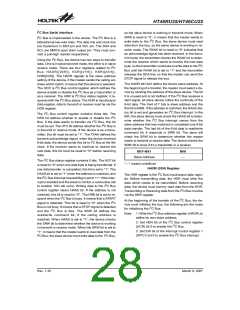
(6+2) PWM Mode
S
Y
S
[
P
W
M
]
=
1
0
0
P
W
M
5
5
5
0
1
1
/
/
/
1
1
1
2
2
2
8
8
8
5
0
/
1
2
8
5
0
/
1
2
8
[
P
W
M
]
=
1
0
1
P
W
M
5
0
/
1
2
8
5
1
/
1
2
8
[
P
W
M
]
=
1
0
2
P
W
M
5
1
/
1
2
8
5
1
/
1
2
8
[
P
W
M
]
=
1
0
3
P
W
M
5
1
/
1
2
8
5
2
/
1
2
8
5
2
/
1
2
8
P
W
M
m
o
d
u
l
a
t
i
o
n
p
e
r
i
o
d
:
1
2
8
/
f
M
o
d
u
l
a
t
i
o
n
c
y
c
l
e
0
M
o
d
u
l
a
t
i
o
n
c
y
c
l
e
1
M
o
d
u
l
a
t
i
o
n
c
y
c
l
e
0
P
W
M
c
y
c
l
e
:
2
5
6
/
f
(7+1) PWM Mode
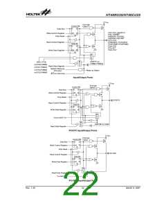
A/D Converter
A/D converter. The bit2~bit0 of the ADCR are used to
select an analog input channel. There are a total of eight
channels to select. The bit5~bit3 of the ADCR are used
to set PB configurations. PB can be an analog input or
as digital I/O line decided by these 3 bits. Once a PB line
is selected as an analog input, the I/O functions and
pull-high resistor of this I/O line are disabled and the A/D
converter circuit is powered on. The EOCB bit (bit6 of
the ADCR) is end of A/D conversion flag. Check this bit
to know when A/D conversion is completed. The START
bit of the ADCR is used to begin the conversion of the
A/D converter. Giving START bit a rising edge and fall-
ing edge means that the A/D conversion has started. In
order to ensure the A/D conversion is completed, the
START should remain at ²0² until the EOCB is cleared to
²0² (end of A/D conversion).
The 8 channels and 12-bit resolution A/D converter are
implemented in this microcontroller. The reference volt-
age is VDD. The A/D converter contains 4 special regis-
ters which are; ADRL (24H), ADRH (25H), ADCR (26H)
and ACSR (27H). The ADRH and ADRL are A/D result
register higher-order byte and lower-order byte and are
read-only. After the A/D conversion is completed, the
ADRH and ADRL should be read to get the conversion
result data. The ADCR is an A/D converter control regis-
ter, which defines the A/D channel number, analog
channel select, start A/D conversion control bit and the
end of A/D conversion flag. If the users want to start an
A/D conversion. Define PB configuration, select the
converted analog channel, and give START bit a raising
edge and falling edge (0®1®0). At the end of A/D con-
version, the EOCB bit is cleared. The ACSR is A/D clock
setting register, which is used to select the A/D clock
source.
Bit 7 of the ACSR register is used for test purposes only
and must not be used for other purposes by the applica-
tion program. Bit1 and bit0 of the ACSR register are
used to select the A/D clock source.
The A/D converter control register is used to control the
Rev. 1.30
24
March 9, 2007

 HOLTEK [ HOLTEK SEMICONDUCTOR INC ]