HT46RU25/HT46CU25
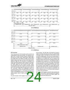
The I/O functions of PA3 are shown below.
of the PWM counter comes from fSYS. The PWM regis-
ters are four 8-bit registers. The waveforms of the PWM
outputs are as shown. Once the PD0/PD1/PD2/PD3 are
selected as the PWM outputs and the output function of
the PD0/PD1/PD2/PD3 are enabled (PDC.0/PDC.1/
PDC.2/PDC.3 =²0²), writing ²1² to PD0/PD1/PD2/PD3
data register will enable the PWM output function and
writing ²0² will force the PD0/PD1/PD2/PD3 to remain
at ²0².
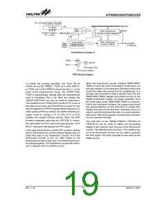
I/O
I/P
O/P
I/P
O/P
Mode (Normal) (Normal)
(PFD)
(PFD)
Logical
Input
Logical
Output
Logical
Input
PFD
PA3
(Timer on)
Note: The PFD frequency is the timer/event counter
overflow frequency divided by 2.
The definitions of PFD control signal and PFD output
frequency are listed in the following table.
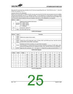
A (6+2) bits mode PWM cycle is divided into four modu-
lation cycles (modulation cycle 0~modulation cycle 3).
Each modulation cycle has 64 PWM input clock period.
In a (6+2) bit PWM function, the contents of the PWM
register is divided into two groups. Group 1 of the PWM
register is denoted by DC which is the value of
PWM.7~PWM.2. The group 2 is denoted by AC which is
the value of PWM.1~PWM.0.
Timer
PA3
PA3
Pad
PFD
Timer Preload
Data
Frequency
Value Register State
Off
Off
On
On
X
X
N
N
0
1
0
1
0
U
X
X
0
X
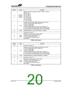
In a (6+2) bits mode PWM cycle, the duty cycle of each
modulation cycle is shown in the table.
PFD
f
TMR/[2´(m-n)]
Parameter
AC (0~3)
Duty Cycle
Note:
²X² stands for unused
²U² stands for unknown
DC+1
64
i<AC
²M² is ²65536² for Timer0, Timer1 PFD,
²256² for Timer2 PFD
Modulation cycle i
(i=0~3)
DC
64
i³AC
²N² is preload value for timer/event counter
²fTMR² is the input clock frequency for the
timer/event counter
A (7+1) bits mode PWM cycle is divided into two modu-
lation cycles (modulation cycle0~modulation cycle 1).
Each modulation cycle has 128 PWM input clock period.
The PB can also be used as A/D converter inputs. The
A/D function will be described later. There is a PWM
function shared with PD0/PD1/PD2/PD3. If the PWM
function is enabled, the PWM0/PWM1/PWM2/PWM3
signal will appear on PD0/PD1/PD2/PD3 (if PD0/PD1/
PD2/PD3 is operating in output mode). The I/O func-
tions of PD0/PD1/PD2/PD3 are as shown.
In a (7+1) bits PWM function, the contents of the PWM
register is divided into two groups. Group 1 of the PWM
register is denoted by DC which is the value of
PWM.7~PWM.1. The group 2 is denoted by AC which is
the value of PWM.0.
In a (7+1) bits mode PWM cycle, the duty cycle of each
modulation cycle is shown in the table.
I/O
I/P
O/P
I/P
O/P
Mode (Normal) (Normal) (PWM)
(PWM)
Parameter
AC (0~1)
Duty Cycle
PD0
PWM0
PWM1
PWM2
PWM3
PD1
PD2
PD3
Logical
Input
Logical
Output
Logical
Input
DC+1
128
i<AC
Modulation cycle i
(i=0~1)
DC
i³AC
128
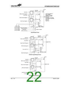
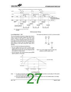
It is recommended that unused or not bonded out I/O
lines should be set as output pins by software instruction
to avoid consuming power under input floating state.
The modulation frequency, cycle frequency and cycle
duty of the PWM output signal are summarized in the
following table.
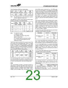
PWM
The microcontroller provides 4 channels (6+2)/(7+1)
(depending on options) bits PWM output shared with
PD0/PD1/PD2/PD3. The PWM channels have their data
registers denoted as PWM0 (1AH), PWM1 (1BH),
PWM2 (1CH) and PWM3 (1DH). The frequency source
PWM
PWM Cycle PWM Cycle
Modulation Frequency
Frequency
Duty
f
f
/64 for (6+2) bits mode
/128 for (7+1) bits mode
SYS
f /256
SYS
[PWM]/256
SYS
Rev. 1.30
23
March 9, 2007

 HOLTEK [ HOLTEK SEMICONDUCTOR INC ]