HT46RU25/HT46CU25
M
i
n
i
m
u
m
o
n
e
i
n
s
t
r
u
c
t
i
o
n
c
y
c
l
e
n
e
e
d
e
d
,
M
a
x
i
m
u
m
t
e
n
i
n
s
t
r
u
c
t
i
o
n
c
y
c
l
e
s
a
l
l
o
w
e
d
S
T
A
R
T
E
O
C
B
A
/
D
s
a
m
p
l
i
n
g
t
i
m
e
A
/
D
s
a
m
p
l
i
n
g
t
i
m
e
A
/
D
s
a
m
p
l
i
n
g
t
i
m
e
t
A
D
C
S
t
A
D
C
S
t
A D C S
P
C
R
2
~
0
0
0
B
1
0
0
B
1
0
1
B
0
0
0
B
1
0
0
B
P
C
R
0
1
.
P
B
p
o
r
t
s
e
t
u
p
a
s
I
/
O
s
2
.
A
t
/
D
c
o
n
v
e
r
t
e
r
i
s
p
o
w
e
r
e
d
o
f
f
o
r
e
d
u
c
e
p
o
w
e
r
c
o
n
s
u
m
p
t
i
o
n
A
C
S
2
~
d
o
n
'
t
c
a
r
e
0
0
0
B
0
0
0
B
0
0
1
B
0
1
0
B
A
C
S
0
P
o
w
e
r
-
o
n
S
t
a
r
t
o
f
A
/
D
S
t
a
r
t
o
f
A
/
D
S
t
a
r
t
o
f
A
/
D
R
e
s
e
t
c
o
n
v
e
r
s
i
o
n
c
o
n
v
e
r
s
i
o
n
c
o
n
v
e
r
s
i
o
n
R
e
s
e
t
A
/
D
R
e
s
e
t
A
/
D
R
e
s
e
t
A
/
D
c
o
n
v
e
r
t
e
r
c
o
n
v
e
r
t
e
r
c
o
n
v
e
r
t
e
r
E
n
d
o
f
A
/
D
E
n
d
o
f
A
/
D
E
n
d
o
f
A
/
D
c
o
n
v
e
r
s
i
o
n
c
o
n
v
e
r
s
i
o
n
c
o
n
v
e
r
s
i
o
n
1
:
D
e
f
i
n
e
P
B
c
o
n
f
i
g
u
r
a
t
i
o
n
2
:
S
e
l
e
c
t
a
n
a
l
o
g
c
h
a
n
n
e
l
t
A
D
C
t
A
D
C
t
A D C
A
/
D
c
o
n
v
e
r
s
i
o
n
t
i
m
e
A
/
D
c
o
n
v
e
r
s
i
o
n
t
i
m
e
A
/
D
c
o
n
v
e
r
s
i
o
n
t
i
m
e
N
o
t
e
:
A
t
t
/
D
c
l
o
c
k
m
u
s
t
b
e
f
S
Y
S
S
Y
S
S
Y
S
A
D
C
S
A
D
A
D
C
A
D
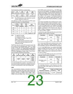
A/D Conversion Timing
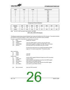
Low Voltage Reset - LVR
The relationship between VDD and VLVR is shown below.
The microcontroller provides low voltage reset circuit in
order to monitor the supply voltage of the device. If the
supply voltage of the device is within the range
0.9V~VLVR, such as changing a battery, the LVR will au-
tomatically reset the device internally. The LVR has the
same effect or function with the external RES signal
which performs a chip reset. During HALT state, LVR is
disabled.
V
D
D
V
O P R
5
.
5
V
5
.
5
V
V
L
V
R
3
.
0
V
2
.
2
V
The LVR includes the following specifications:
·
The low voltage (0.9V~VLVR) has to remain in their
original state for more than 1ms. If the low voltage
state does not exceed 1ms, the LVR will ignore it and
do not perform a reset function.
0
.
9
V
Note: VOPR is the voltage range for proper chip
operation at 4MHz system clock.
·
The LVR uses the ²OR² function with the external RES
signal to perform a chip reset.
V
D
D
5
.
5
V
L
V
R
D
e
t
e
c
t
V
o
l
t
a
g
e
V
L
V
R
0
.
9
0
V
V
R
e
s
e
t
S
i
g
n
a
l
R
e
s
e
t
N
o
r
m
a
l
O
p
e
r
a
t
i
o
n
R
e
s
e
t
*
1
*
2
Low Voltage Reset
Note: *1: To make sure that the system oscillator has stabilized, the SST provides an extra delay of 1024 system
clock pulses before entering the normal operation.
*2: Since low voltage state has to be maintained in its original state for over 1ms, therefore after a 1ms delay,
the device enters the reset mode.
Rev. 1.30
27
March 9, 2007

 HOLTEK [ HOLTEK SEMICONDUCTOR INC ]