HT46RU25/HT46CU25
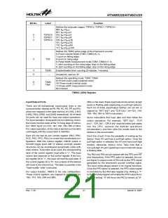
Bit No.
Label
Function
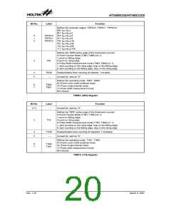
Defines the prescaler stages, T2PSC2, T2PSC1, T2PSC0=
000: fINT=fSYS
001: fINT=fSYS/2
0
1
2
T2PSC0
T2PSC1
T2PSC2
010: fINT=fSYS/4
011: fINT=fSYS/8
100: fINT=fSYS/16
101: fINT=fSYS/32
110: fINT=fSYS/64
111: fINT=fSYS/128
Defines the TMR2 active edge of the timer/event counter:
In Event Counter Mode (T2M1,T2M0)=(0,1):
1:count on falling edge;
3
T2E
0:count on rising edge
In Pulse Width measurement mode (T2M1,T2M0)=(1,1):
1: start counting on the rising edge, stop on the falling edge;
0: start counting on the falling edge, stop on the rising edge
4
5
T2ON
Enable/disable timer counting (0=disable; 1=enable)
¾
Unused bit, read as ²0²
Defines the operating mode, T2M1, T2M0:
01=Event count mode (external clock)
10=Timer mode (internal clock)
11=Pulse width measurement mode
00=Unused
6
7
T2M0
T2M1
TMR2C (2EH) Register
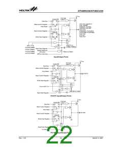
Input/Output Ports
After a chip reset, these input/output lines remain at high
levels or floating state (depending on pull-high options).
Each bit of these input/output latches can be set or
cleared by ²SET [m].i² and ²CLR [m].i² (m=12H, 14H,
16H, 18H, 28H or 2AH) instructions.
There are 48 bidirectional input/output lines in the
microcontroller, labeled as PA, PB, PC, PD, PF and PG,
which are mapped to the data memory of [12H], [14H],
[16H], [18H], [28H] and [2AH] respectively. All of these
I/O ports can be used for input and output operations.
For input operation, these ports are non-latching, that is,
the inputs must be ready at the T2 rising edge of instruc-
tion ²MOV A,[m]² (m=12H, 14H, 16H, 18H, 28H or 2AH).
For output operation, all the data is latched and remains
unchanged until the output latch is rewritten.
Some instructions first input data and then follow the
output operations. For example, ²SET [m].i², ²CLR
[m].i², ²CPL [m]², ²CPLA [m]² read the entire port states
into the CPU, execute the defined operations
(bit-operation), and then write the results back to the
latches or the accumulator.
Each I/O line has its own control register (PAC, PBC,
PCC, PDC, PFC, PGC) to control the input/output con-
figuration. With this control register, CMOS output or
Schmitt trigger input with or without pull-high resistor
structures can be reconfigured dynamically under soft-
ware control. To function as an input, the corresponding
latch of the control register must write a ²1². The input
source also depends on the control register. If the con-
trol register bit is ²1², the input will read the pad state. If
the control register bit is ²0², the contents of the latches
will move to the internal bus. The latter is possible in the
²read-modify- write² instruction.
Each line of port A has the capability of waking-up the
device. Each I/O port has a pull-high option. Once the
pull-high option is selected, the I/O port has a pull-high
resistor, otherwise, there¢s none. Take note that a
non-pull-high I/O port operating in input mode will cause
a floating state.
The PA3 and PA5 are pin-shared with the PFD and INT
pins respectively. If the PFD option is selected, the out-
put signal in output mode of PA3 will be the PFD signal
generated by the timer/event counter overflow signal.
The input mode always remain in its original functions.
Once the PFD option is selected, the PFD output signal
is controlled by the PA3 data register only. Writing a ²1²
to the PA3 data register will enable the PFD output func-
tion and writing ²0² will force the PA3 to remain at ²0².
For output function, CMOS is the only configuration.
These control registers are mapped to locations 13H,
15H, 17H, 19H, 29H and 2BH.
Rev. 1.30
21
March 9, 2007

 HOLTEK [ HOLTEK SEMICONDUCTOR INC ]