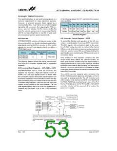
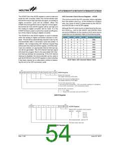
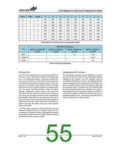
HT37B90/HT37B70/HT37B50/HT37B30
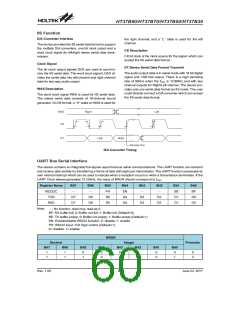
SPI Serial Interface
There are two SPI interfaces, with each interface containing four basic signals and pins. These are SDI (serial data in-
put), SDO (serial data output), SCK (serial clock) and SCS (slave select pin).
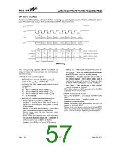
SPI Timing
¨
Bit3 (MLS) ® MSB or LSB (1/0) shift first control bit
Two corresponding registers, SBCR and SBDR are
unique to the serial interface and provide control, status,
and data storage.
¨
Bit2 (CSEN) ® serial bus selection signal enable/dis-
able (SCS), when CSEN=0, SCSB is floating.
¨
·
Bit1 (WCOL) ® this bit is set to 1 if data is written to
the SBDR register (TXRX buffer) when data is
transferred, writing will be ignored if data is written
to SBDR (TXRX buffer) when data is transferred.
SBCR: Serial bus control register
¨
Bit7 (CKS) clock source selection: fSIO=fOSC/2,
select as ²0². fSIO=fOSC, select as ²1².
¨
Bit6 (M1), Bit5 (M0) master/slave mode and baud
rate selection
¨
Bit0 (TRF) ® data transferred or data received
used to generate an interrupt.
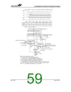
M1, M0:
Note: data reception is still in operation when the MCU
enters the Power-down mode.
00 ® MASTER MODE, BAUD RATE= fSIO
01 ® MASTER MODE, BAUD RATE= fSIO/4
10 ® MASTER MODE, BAUD RATE= fSIO/16
11 ® SLAVE MODE
·
SBDR: Serial bus data register
Data written to SBDR ® write data to the TXRX buffer
only
¨
Bit4 (SBEN) ® serial bus enable/disable (1/0)
Data read from SBDR ® read from SBDR only
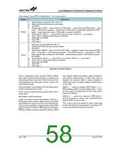
Operating Mode description:
-
Enable: (SCS dependent on CSEN bit)
Disable ® enable: SCK, SDI, SDO, SCS= 0
(SCK= ²0²) and waiting for writing data to SBDR
(TXRX buffer)
Master transmitter: clock transmission and data I/O
started by writing to SBDR
Master clock transmission initiated by writing to SBDR
Slave transmitter: data I/O started by clock reception
Slave receiver: data I/O started by clock reception
Master mode: write data to SBDR (TXRX buffer)
start transmission/reception automatically
Master mode: when the data has been trans-
ferred, set TRF
Slave mode: when an SCK (and SCS dependent
on CSEN) is received, data in the TXRX buffer is
shifted-out and data on SDI is shifted-in.
-
Disable: SCK (SCK), SDI, SDO, SCS floating
Rev. 1.00
57
June 22, 2017

 HOLTEK [ HOLTEK SEMICONDUCTOR INC ]