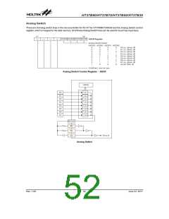
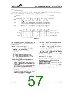
HT37B90/HT37B70/HT37B50/HT37B30
·
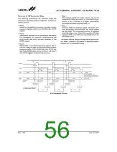
Summary of A/D Conversion Steps
Step 4
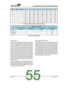
The analog to digital conversion process can now be
initialised by setting the START bit in the ADCR regis-
ter from ²0² to ²1² and then to ²0² again. Note that this
bit should have been originally set to ²0².
The following summarizes the individual steps that
should be executed in order to implement an A/D con-
version process.
·
Step 1
·
Step 5
Select the required A/D conversion clock by correctly
programming bits ADCS1 and ADCS0 in the ACSR
register.
To check when the analog to digital conversion pro-
cess is complete, the EOCB bit in the ADCR register
can be polled. The conversion process is complete
when this bit goes low. When this occurs the A/D data
registers ADRL and ADRH can be read to obtain the
conversion value.
·
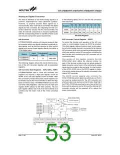
Step 2
Select which channel is to be connected to the internal
A/D converter by correctly programming the
ACS2~ACS0 bits which are also contained in the
ADCR register.
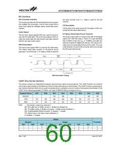
The following timing diagram shows graphically the vari-
ous stages involved in an analog to digital conversion
process and its associated timing.
·
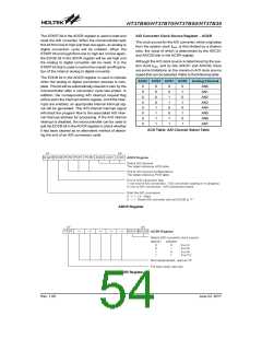
Step 3
Select which pins on Port B are to be used as A/D in-
puts and configure them as A/D input pins by correctly
programming the PCR2~PCR0 bits in the ADCR reg-
ister. Note that this step can be combined with Step 2
into ADCR registers programming operation.
A/D Conversion Timing
Rev. 1.00
56
June 22, 2017

 HOLTEK [ HOLTEK SEMICONDUCTOR INC ]