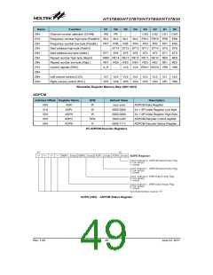
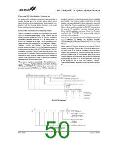
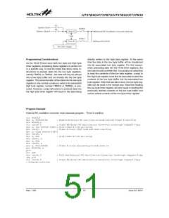
HT37B90/HT37B70/HT37B50/HT37B30
Analog to Digital Converter
The need to interface to real world analog signals is a
common requirement for many electronic systems.
However, to properly process these signals by a
microcontroller, they must first be converted into digital
signals by A/D converters. By integrating the A/D con-
version electronic circuitry into the microcontroller, the
need for external components is reduced significantly
with the corresponding follow-on benefits of lower costs
and reduced component space requirements.
In the following tables, D0~D11 are the A/D conversion
data result bits.
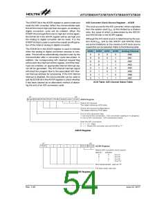
Bit Bit Bit Bit Bit Bit Bit Bit
Register
7
6
5
4
3
2
1
0
ADRL
D3 D2 D1 D0
¾
¾
¾
¾
ADRH D11 D10 D9 D8 D7 D6 D5 D4
A/D Data Register
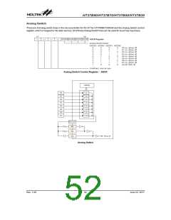
A/D Converter Control Register - ADCR
A/D Overview
To control the function and operation of the A/D con-
verter, a control register known as ADCR is provided.
This 8-bit register defines functions such as the selec-
tion of which analog channel is connected to the internal
A/D converter, which pins are used as analog inputs and
which are used as normal I/Os as well as controlling the
start function and monitoring the A/D converter end of
conversion status.
HT37B90/70/50/30 contains a 8-channel analog to digi-
tal converter which can directly interface to external an-
alog signals, such as that from sensors or other control
signals and convert these signals directly into either a
12-bit digital value.
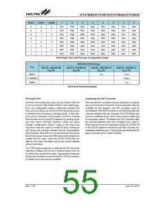
Input
Conversion
Bits
Device
Input Pins
Channels
HT37B90/70,
HT37B50/30
8
12
PB0~PB7
One section of this register contains the bits
ACS2~ACS0 which define the channel number. As
each of the devices contains only one actual analog to
digital converter circuit, each of the individual 8 analog
inputs must be routed to the converter. It is the function
of the ACS2~ACS0 bits in the ADCR register to deter-
mine which analog channel is actually connected to the
internal A/D converter.
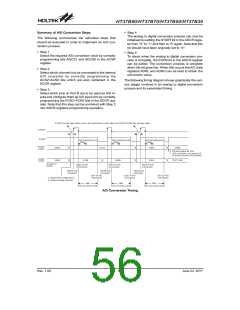
The following diagram shows the overall internal struc-
ture of the A/D converter, together with its associated
registers.
A/D Converter Data Registers - ADR, ADRL, ADRH
HT37B90/70/50/30 have a 12-bit A/D converter, two
registers are required, a high byte register, known as
ADRH, and a low byte register, known as ADRL. After
the conversion process takes place, these registers can
be directly read by the microcontroller to obtain the digi-
tized conversion value. HT37B90/70/50/30 use two A/D
Converter Data Registers, note that only the high byte
register ADRH utilizes its full 8-bit contents. The low
byte register utilizes only 4 bit of its 8-bit contents as it
contains only the lower 4 bit of the 12-bit converted
value.
The ADCR control register also contains the
PCR2~PCR0 bits which determine which pins on Port A
are used as analog inputs for the A/D converter and
which pins are to be used as normal I/O pins. Note that if
the PCR2~PCR0 bits are all set to zero, then all the Port
B pins will be setup as normal I/Os and the internal A/D
converter circuitry will be powered off to reduce the
power consumption.
A/D Converter Structure
Rev. 1.00
53
June 22, 2017

 HOLTEK [ HOLTEK SEMICONDUCTOR INC ]