HT37B90/HT37B70/HT37B50/HT37B30
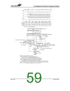
Clock polarity= rising (SCK) or falling (SCK): 1 or 0 (mask option).
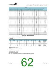
Modes
Operations
1. Select CKS and select M1, M0 = 00,01,10
2. Select CSEN, MLS (the same as the slave)
3. Set SBEN
4. Writing data to SBDR ® data is stored in TXRX buffer ® output SCK (and SCS) signals ® go to
step 5 ® (SIO internal operation ® data stored in TXRX buffer, and SDI data is shifted into TXRX
buffer ® data transferred, data in TXRX buffer is latched into SBDR)
5. Check WCOL; WCOL= 1 ® clear WCOL and go to step 4; WCOL= 0 ® go to step 6
6. Check TRF or waiting for SBI (serial bus interrupt)
7. Read data from SBDR
Master
8. Clear TRF
9. Go to step 4
1. CKS don¢t care and select M1, M0= 11
2. Select CSEN, MLS (the same as the master)
3. Set SBEN
4. Writing data to SBDR ® data is stored in TXRX buffer ® waiting for master clock signal (and SCS):
SCK ® go to step 5 ® (SIO internal operations ® SCK (SCS) received ® output data in TXRX
buffer and SDI data is shifted into TXRX buffer ® data transferred, data in TXRX buffer is latched
into SBDR)
Slave
5. Check WCOL; WCOL= 1 ® clear WCOL, go to step 4; WCOL= 0 ® go to step 6
6. Check TRF or wait for SBI (serial bus interrupt)
7. Read data from SBDR
8. Clear TRF
9. Go to step 4
Operation of Serial Interface
WCOL: master/slave mode, set while writing to SBDR
when data is transferring (transmitting or receiving) and
this writing will then be ignored. WCOL function can be
enabled/disabled by mask option. WCOL is set by SIO
and cleared by users.
has 2 options: CSEN mask option is used to enable/dis-
able software CSEN function. If CSEN mask option is
disabled, the software CSEN is always disabled. If
CSEN mask option is enabled, software CSEN function
can be used.
Data transmission and reception are still working when
the MCU enters the HALT mode.
SBEN= 1 ® serial bus standby; SCS (CSEN= 1) = 1;
SCS= floating (CSEN= 0); SDI= floating; SDO= 1; mas-
ter SCK= output 1/0 (dependent on CPOL mask option),
slave SCK= floating.
CPOL is used to select the clock polarity of SCK. It is a
mask option.
SBEN= 0 ® serial bus disabled; SCS=SDO=1,
SDI=SCK= floating in master mode, SDI=SDO=SCK=
floating, SCS=1 in slave mode.
MLS: MSB or LSB first selection.
CSEN: chip select function enable/disable, CSEN=1 ®
SCS signal function is active. Master should output SCS
signal before SCL signal is set and slave data transfer-
ring should be disabled (or enabled) before (after) SCS
signal is received. CSEN= 0, SCS signal is not needed,
SCS pin (master and slave) should be floating. CSEN
TRF is set by SIO and cleared by users. When data
transfer (transmission and reception) is completed, TRF
is set to generate SBI (serial bus interrupt).
Rev. 1.00
58
June 22, 2017

 HOLTEK [ HOLTEK SEMICONDUCTOR INC ]