HT37B90/HT37B70/HT37B50/HT37B30
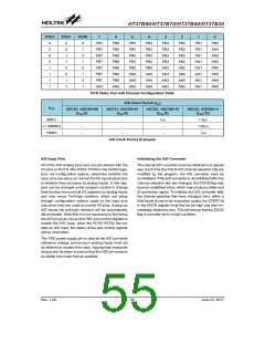
PCR2
PCR1
PCR0
7
6
5
4
3
2
1
0
0
0
0
0
1
1
1
1
0
0
1
1
0
0
1
1
0
1
0
1
0
1
0
1
PB7
PB7
PB7
PB7
PB7
PB7
PB7
AN7
PB6
PB6
PB6
PB6
PB6
PB6
PB6
AN6
PB5
PB5
PB5
PB5
PB5
AN5
AN5
AN5
PB4
PB4
PB4
PB4
PB4
AN4
AN4
AN4
PB3
PB3
PB3
PB3
AN3
AN3
AN3
AN3
PB2
PB2
PB2
AN2
AN2
AN2
AN2
AN2
PB1
PB1
AN1
AN1
AN1
AN1
AN1
AN1
PB0
AN0
AN0
AN0
PB0
AN0
AN0
AN0
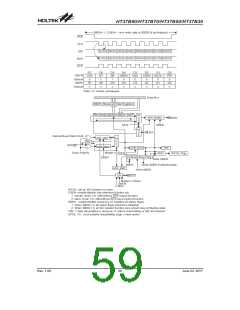
PCR Table: Port A/D Channel Configuration Table
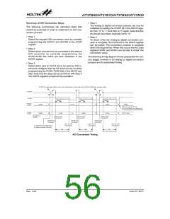
A/D Clock Period (tAD
)
fOSC
ADCS1, ADCS0=00
(fOSC/4)
ADCS1, ADCS0=01
(fOSC/6)
ADCS1, ADCS0=10
(fOSC/8)
ADCS1, ADCS0=11
(fOSC/12)
8MHz
11.059MHz
12MHz
¾
¾
¾
¾
¾
¾
1ms
¾
1.5ms
1.08ms
1ms
¾
A/D Clock Period Examples
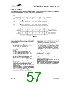
A/D Input Pins
Initialising the A/D Converter
All of the A/D analog input pins are pin-shared with the
I/O pins on Port B. Bits PCR2~PCR0 in the ACSR regis-
ters, not configuration options, determine whether the
input pins are setup as normal Port B input/output pins
or whether they are setup as analog inputs. In this way,
pins can be changed under program control to change
their function from normal I/O operation to analog inputs
and vice versa. Pull-high resistors, which are setup
through configuration options, apply to the input pins
only when they are used as normal I/O pins, if setup as
A/D inputs the pull-high resistors will be automatically
disconnected. Note that it is not necessary to first setup
the A/D pin as an input in the PBC port control register to
enable the A/D input, when the PCR2~PCR0 bits en-
able an A/D input, the status of the port control register
will be overridden.
The internal A/D converter must be initialized in a special
way. Each time the Port B A/D channel selection bits are
modified by the program, the A/D converter must be
re-initialised. If the A/D converter is not initialized after the
channel selection bits are changed, the EOCB flag may
have an undefined value, which may produce a false end
of conversion signal. To initialize the A/D converter after
the channel selection bits have changed, then, within a
time frame of one to ten instruction cycles, the START bit
in the ADCR register must first be set high and then im-
mediately cleared to zero. This will ensure that the EOCB
flag is correctly set to a high condition.
The VDD power supply pin is used as the A/D converter
reference voltage, and as such analog inputs must not
be allowed to exceed this value. Appropriate measures
should also be taken to ensure that the VDD pin remains
as stable and noise free as possible.
Rev. 1.00
55
June 22, 2017

 HOLTEK [ HOLTEK SEMICONDUCTOR INC ]