HT37B90/HT37B70/HT37B50/HT37B30
·
A/D Inputs
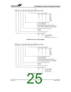
I/O Pin Structures
The HT37B90/70/50/30 have 8 A/D converter channel
inputs. All of these analog inputs are pin-shared with
PB0 to PB7. If these pins are to be used as A/D inputs
and not as normal I/O pins then the corresponding bits
in the A/D Converter Control Register, ADCR.3~5 and
ADSR.4, must be properly set. There are no configu-
ration options associated with the A/D function. If
used as I/O pins, then full pull-high resistor selections
remain, however if used as A/D inputs then any
pull-high resistor selections associated with these
pins will be automatically disconnected.
The diagrams illustrate the I/O pin internal structures. As
the exact logical construction of the I/O pin may differ
from these drawings, they are supplied as a guide only
to assist with the functional understanding of the I/O
pins.
Programming Considerations
Within the user program, one of the first things to con-
sider is port initialization. After a reset, the PA~PE data
register and PAC~PEC port control register will be set
high. This means that all I/O pins will default to an input
state, the level of which depends on the other connected
circuitry and whether pull-high options have been se-
lected. If the PAC port control register, is then pro-
grammed to setup some pins as outputs, these output
pins will have an initial high output value unless the as-
sociated PA port data register is first programmed. Se-
lecting which pins are inputs and which are outputs can
be achieved byte-wide by loading the correct value into
the port control register or by programming individual
bits in the port control register using the ²SET [m].i² and
²CLR [m].i² instructions.
·
CR/F analog switch Inputs
The HT37B90/70/50/30 have 8 CR/F converter in-
puts. All of these analog inputs are pin-shared with
PC0 to PC7. If these pins are to be used as CR/F ana-
log switch Inputs and not as normal I/O pins then the
corresponding bits in the Option, ²PC0~7 share pin
configuration². All of these analog inputs are
pin-shared with PC0 to PC7. If these pins are to be
used as CR/F analog switch Inputs and not as normal
I/O pins then the corresponding bits in the configura-
tion, ²PC0~7 share pin configuration².
·
·
·
CR/F oscillator pin
The HT37B90/70/50/30 have 4 CR/F oscillator pins. All
of these CR/F oscillator pin are pin-shared with PD0 to
PD3. If these pins are to be used as CR/F oscillator
pins and not as normal I/O pins then the corresponding
bits in the Option, ²PD0~3 share pin Option².
Note that when using these bit control instructions, a
read-modify-write operation takes place. The
microcontroller must first read in the data on the entire
port, modify it to the required new bit values and then re-
write this data back to the output ports.
UART pin
The device have 3 UART pins. All of these UART pins
are pin-shared with PE0 to PE2. If these pins are to be
used as UART pins and not as normal I/O pins then
the corresponding bits in the PE share pin configura-
tion option.
SPI pin
The device have 4 SPI pins. All of these SPI pins are
pin-shared with PE3 to PE6. If these pins are to be
used as SPI pins and not as normal I/O pins then the
corresponding bits in the PE share pin configuration
option.
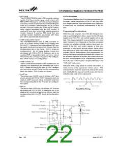
Read/Write Timing
Input/Output Port
Rev. 1.00
22
June 22, 2017

 HOLTEK [ HOLTEK SEMICONDUCTOR INC ]