HT37B90/HT37B70/HT37B50/HT37B30
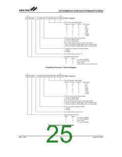
SPI Registers - SBCR, SBDR
Various methods exist to wake-up the microcontroller,
one of which is to change the logic condition on one of
the PA0~PA7 pins from high to low. After a HALT instruc-
tion forces the microcontroller into entering the Power
Down Mode, the processor will remain idle or in a
low-power state until the logic condition of the selected
wake-up pin on Port A changes from high to low. This
function is especially suitable for applications that can
be woken up via external switches. Note that pins PA0 to
PA7 can be selected individually to have this wake-up
feature using an PA wake up option, located in the con-
figuration.
The device contain an internal SPI function which is
controlled via these two registers. The SBCR is the sta-
tus and control register for the SPI function. The actual
data that is to be transmitted or that is received on the
serial interface is stored in the SBDR register.
UART Registers - RS232C, TXD, RXD, BRGR
The device contain an internal UART function which is
controlled via these four registers. The RS232C is the
status and control register for the UART .The actual data
that is to be transmitted or that is received on the serial
interface is stored in the TXD/RXD register. The BRGR
register set to generates UART baud rate clock
31.25kHz according to fOSC.
I/O Port Control Registers
Each I/O port have their own control register, known as
PAC, PBC, PCC, PDC and PEC, which control the in-
put/output configuration. With this control register, each
PA~PE I/O pin with or without pull-high resistors can be
reconfigured by pull-hi option control. Pins PA~PE ports
are directly mapped to a bit in its associated port control
register. For the I/O pin to function as an input, the corre-
sponding bit of the control register must be written as a
²1². This will then allow the logic state of the input pin to
be directly read by instructions. When the correspond-
ing bit of the control register is written as a ²0², the I/O
pin will be setup as a CMOS output. If the pin is currently
setup as an output, instructions can still be used to read
the output register.
Input/Output Ports
Holtek microcontrollers offer considerable flexibility on
their I/O ports. With the input or output designation of ev-
ery pin fully under user program control, pull-high op-
tions for all ports and wake-up options on certain pins,
the user is provided with an I/O structure to meet the
needs of a wide range of application possibilities. De-
pending upon which device or package is chosen, the
microcontroller range provides from 32 to 40
bidirectional input/output lines labeled with port names
PA, PB, PC, PD and PE. These I/O ports are mapped to
the RAM Data Memory with specific addresses as
shown in the Special Purpose Data Memory table. All of
these I/O ports can be used for input and output opera-
tions. For input operation, these ports are non-latching,
which means the inputs must be ready at the T2 rising
edge of instruction ²MOV A,[m]², where m denotes the
port address.
However, it should be noted that the program will in fact
only read the status of the output data latch and not the
actual logic status of the output pin.
·
Pin-shared Functions
The flexibility of the microcontroller range is greatly
enhanced by the use of pins that have more than one
function. Limited numbers of pins can force serious
design constraints on designers but by supplying pins
with multi-functions, many of these difficulties can be
overcome. For some pins, the chosen function of the
multi-function I/O pins is set by configuration options
while for others the function is set by application pro-
gram control.
For output operation, all the data is latched and remains
unchanged until the output latch is rewritten.
Pull-high Resistors
Many product applications require pull-high resistors for
their switch inputs usually requiring the use of an exter-
nal resistor. To eliminate the need for these external re-
sistors, I/O pins PA~PE, when configured as an input
have the capability of being connected to an internal
pull-high resistor. These pull-high resistors are
selectable via PA~PE option respectively, located in the
configuration. The pull-high resistors are implemented
using weak PMOS transistors.
·
External Interrupt Input
The external interrupt pin, INT, is pin-shared with the
I/O pin PA5. To use the pin as an external interrupt in-
put the correct bits in the PA share pin option must be
selected. The pin must also be setup as an input by
setting the appropriate bit in the Port Control Register.
A pull-high resistor can also be selected via the appro-
priate port pull-high option.
Port A Wake-up
If the HALT instruction is executed, the device will enter
the Power Down Mode, where the system clock will stop
resulting in power being conserved, a feature that is im-
portant for battery and other low-power applications.
Rev. 1.00
21
June 22, 2017

 HOLTEK [ HOLTEK SEMICONDUCTOR INC ]