HT36B0
Wavetable ROM
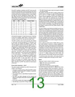
(TMR1H;0FH), the Timer/event Counter 1 Lower-order
byte register (TMR1L;10H), the Timer/event Counter 1
Control register (TMR1C;11H), the I/O registers
(PA;12H, PB;14H, PC;16H, PD;18H, PE;1AH), the pro-
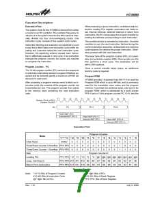
The ST15~0 is used to defined the start address of each
sample on the wavetable and read the waveform data
from the location. HT36B0 provides 21 output address
lines from WA17~0, the ST15~0 is used to locate the
major 16 bits of 21 lines and the undefined data from
WA4~0 is always set to 00000b. So the start address of
each sample have to be located at a multiple of 32. Oth-
erwise, the sample will not be read out correctly be-
cause it has a wrong starting code.
0
0
0
1
H
H
I
n
d
i
r
e
c
t
A
d
d
r
e
s
s
i
n
g
R
e
g
i
s
t
e
r
0
M
P
0
0
2
H
I
n
d
i
r
e
c
t
A
d
d
r
e
s
s
i
n
g
R
e
g
i
s
t
e
r
1
0
3
H
M
P
1
0
4
H
B
P
0
5
H
A
C
C
P
C
L
0
6
H
T
B
L
P
0
7
H
Stack Register - Stack
T
B
L
H
0
8
H
W
D
T
S
0
9
H
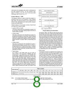
This is a special part of the memory which is used to
save the contents of the program counter (PC) only. The
stack is organized into 8 levels and is neither part of the
data nor part of the program space, and is neither read-
able nor writeable. The activated level is indexed by the
stack pointer (SP) and is neither readable nor writeable.
At a subroutine call or interrupt acknowledgment, the
contents of the program counter are pushed onto the
stack. At the end of a subroutine or an interrupt routine,
signaled by a return instruction (RET or RETI), the pro-
gram counter is restored to its previous value from the
stack. After a chip reset, the SP will point to the top of the
stack.
S
T
A
T
U
S
0
0
A
B
H
H
I
N
T
C
T
M
R
0
H
0
C
H
T
M
R
0
L
0
D
H
S
D
p
e
c
i
a
l
P
u
r
p
o
s
e
T
T
M
M
R
R
0
1
C
H
0
E
H
a
t
a
M
e
m
r
o
y
0
F
H
T
M
R
1
L
1
1
0
1
H
H
T
M
R
1
C
P
A
1
2
H
P
A
C
1
3
H
P
B
1
4
H
P
B
C
1
5
H
P
P
C
1
6
H
P
P
C
D
C
C
1
7
H
D
1
1
8
9
H
H
If the stack is full and a non-masked interrupt takes
place, the interrupt request flag will be recorded but the
acknowledgment will be inhibited. When the stack
pointer is decremented (by RET or RETI), the interrupt
will be serviced. This feature prevents stack overflow al-
lowing the programmer to use the structure more easily.
In a similar case, if the stack is full and a CALL is subse-
quently executed, a stack overflow occurs and the first
entry will be lost (only the most recent eight return ad-
dress are stored).
1
1
A
B
H
H
P
E
P
E
C
1
C
H
P
F
1
D
H
D
A
C
H
i
g
h
B
y
t
e
(
D
A
H
)
1
E
H
D
A
C
L
o
w
B
y
t
e
(
D
A
L
)
1
F
H
D
A
C
C
o
n
t
r
o
l
(
D
A
C
)
2
2
0
1
H
H
C
h
a
n
n
e
l
N
u
m
b
e
r
H
S
e
l
e
c
t
(
C
H
A
N
)
F
r
e
q
u
e
n
c
y
N
u
m
b
e
r
i
g
h
B
y
t
e
(
F
r
e
q
N
H
)
2
2
H
F
r
e
q
u
e
n
c
y
N
u
m
b
e
r
L
o
w
B
y
t
e
(
F
r
e
q
N
L
)
2
3
H
S
t
a
r
t
A
d
d
r
e
s
s
H
i
g
h
B
y
t
e
(
A
d
d
r
H
)
2
4
H
S
t
a
r
t
A
d
d
r
e
m
s
s
L
o
w
B
y
t
e
(
A
d
d
r
L
)
W
F
R
a
v
e
t
a
b
l
e
2
5
H
R
e
p
e
a
t
N
u
b
e
r
H
i
g
h
B
y
t
e
(
R
e
H
)
Data Memory - RAM
u
n
c
t
i
o
n
2
6
H
R
e
p
e
a
t
N
u
m
b
e
r
L
o
w
B
y
t
e
(
R
e
L
)
e
g
i
s
t
e
r
The data memory is designed with 4 ´ 256 ´ 8 bits. The
data memory is divided into three functional groups:
special function registers, wavetable function register,
and general purpose data memory (4 ´ 192 ´ 8). Most of
them are read/write, but some are read only.
C
o
n
t
r
o
l
R
e
g
i
s
t
e
r
(
E
N
V
)
2
7
H
2
8
H
L
e
f
t
V
o
l
u
m
e
C
o
n
t
r
o
l
(
L
V
C
)
2
9
H
R
i
g
h
t
V
o
l
u
m
e
C
o
n
t
r
o
l
(
R
V
C
)
2
A
H
R
S
2
3
2
C
2
2
B
C
H
T
X
D
H
H
R
X
D
The special function registers include the Indirect Ad-
dressing register 0/1 (00H/02H), the Memory Pointer
register 0/1 (MP0;01H/MP1;03H), the RAM address
bank pointer (BP;04H), the Accumulator (ACC;05H), the
Program Counter Lower-byte register (PCL;06H), the
Table Pointer (TBLP;07H), the Table Higher-order byte
register (TBLH;08H), the Watchdog Timer option Set-
ting register (WDTS;09H), the Status register
(STATUS;0AH), the Interrupt Control register
(INTC;0BH), the Timer/event Counter 0 Higher-order
byte register (TMR0H;0CH), the Timer/event Counter 0
Lower-order byte register (TMR0L;0DH), the
Timer/event Counter 0 Control register (TMR0C;0EH),
the Timer/ event Counter 1 Higher-order byte register
2
D
I
N
T
C
H
2
2
E
F
H
H
:
U
n
u
s
e
d
.
R
e
a
d
a
s
"
0
0
"
3
F
H
B
a
n
k
3
B
a
n
k
2
B
a
n
k
1
4
0
H
B
a
n
k
0
G
e
n
e
r
a
l
P
u
r
p
o
s
e
D
a
t
a
M
e
m
o
r
y
(
1
9
2
´
4
B
y
t
e
s
)
F
F
H
RAM Mapping
Rev. 1.10
9
July 3, 2008
图片预览")
 HOLTEK [ HOLTEK SEMICONDUCTOR INC ]