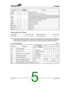
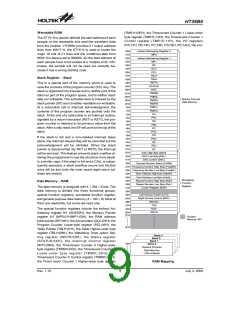
HT36B0
Internal
Connection
Pad Name
I/O
Function
VDDA
VSSA
DAC power supply
Negative power supply of DAC, ground
¾
¾
¾
¾
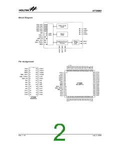
OSC1 and OSC2 are connected to an RC network or a crystal (by mask
option) for the internal system clock. In the case of RC operation, OSC2 is
the output terminal for 1/8 system clock. The system clock may come from
the crystal, the two pins cannot be floating.
OSC1
OSC2
I
¾
O
GND
Negative power supply, ground
Positive power supply
Reset input, active low
MIDI Output
¾
¾
I
¾
¾
¾
¾
¾
¾
VDD
RES
MIDI_OUT
MIDI_THRN
MIDI_IN
O
O
I
MIDI through
MIDI input
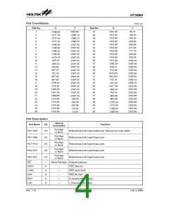
Absolute Maximum Ratings
Supply Voltage .............................VSS-0.3V to VSS+6V
Input Voltage .............................VSS-0.3V to VDD+0.3V
Storage Temperature ...........................-50°C to 125°C
Operating Temperature ..........................-25°C to 70°C
Note: These are stress ratings only. Stresses exceeding the range specified under ²Absolute Maximum Ratings² may
cause substantial damage to the device. Functional operation of this device at other conditions beyond those listed
in the specification is not implied and prolonged exposure to extreme conditions may affect device reliability.
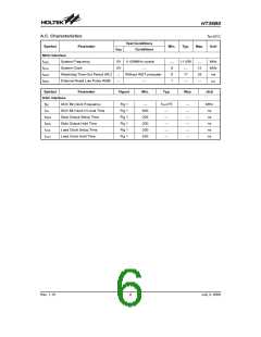
D.C. Characteristics
Ta=25°C
Test Conditions
Symbol
Parameter
Operating Voltage
Min.
Typ.
Max.
Unit
VDD
Conditions
VDD
IDD
3.6
4.5
16
5.5
32
V
¾
¾
No load,
Operating Current
4.5V
mA
¾
fOSC=11.0592MHz
No load,
ISTB
Standby Current (WDT Disabled)
4.5V
1
3
¾
mA
System HALT
IOH
IOL
VOH=4.5V
VOL=0.5V
I/O Ports Source Current
I/O Ports Sink Current
4.5V
4.5V
4.5V
4.5V
5
mA
mA
V
¾
¾
¾
¾
30
¾
¾
5
0.8VDD
0
VIH
VIL
VDD
Input High Voltage for I/O Ports
Input Low Voltage for I/O Ports
¾
¾
0.2VDD
V
RPH
VIL=0V
Pull-High Resistance of I/O Ports (INT) 4.5V
¾
¾
kW
Rev. 1.10
5
July 3, 2008
图片预览")
 HOLTEK [ HOLTEK SEMICONDUCTOR INC ]