HT36B0
Function Description
Execution Flow
When executing a jump instruction, conditional skip ex-
ecution, loading PCL register, subroutine call, initial re-
set, internal interrupt, external interrupt or return from
subroutine, the PC manipulates the program transfer by
loading the address corresponding to each instruction.
The system clock for the HT36B0 is derived from either
a crystal or an RC oscillator. The oscillator frequency di-
vided by 2 is the system clock for the MCU and it is inter-
nally divided into four non-overlapping clocks. One
instruction cycle consists of four system clock cycles.
The conditional skip is activated by instruction. Once the
condition is met, the next instruction, fetched during the
current instruction execution, is discarded and a dummy
cycle replaces it to retrieve the proper instruction. Other-
wise proceed with the next instruction.
Instruction fetching and execution are pipelined in such
a way that a fetch takes one instruction cycle while de-
coding and execution takes the next instruction cycle.
However, the pipelining scheme causes each instruc-
tion to effectively execute in one cycle. If an instruction
changes the program counter, two cycles are required
to complete the instruction.
The lower byte of the program counter (PCL) is a read-
able and writeable register (06H). Moving data into the
PCL performs a short jump. The destination will be
within 256 locations.
Program Counter - PC
Once a control transfer takes place, an additional
dummy cycle is required.
The 13-bit program counter (PC) controls the sequence
in which the instructions stored in program ROM are ex-
ecuted and its contents specify a maximum of 8192 ad-
dresses for each bank.
Program ROM
HT36B0 provides 18 address lines WA17~0 to read the
Program ROM which is up to 4M bits, and is commonly
used for the wavetable voice codes and the program
memory. It provides two address types, one type is for
program ROM, which is addressed by a bank pointer
PF4~0 and a 13-bit program counter PC 12~0; and the
After accessing a program memory word to fetch an in-
struction code, the contents of the program counter are
incremented by one. The program counter then points
to the memory word containing the next instruction
code.
T
1
T
2
T
3
T
4
T
1
T
2
T
3
T
4
T
1
T
2
T
3
T
4
S
y
s
t
e
m
C
l
o
c
k
o
f
M
C
U
(
S
y
s
t
e
m
C
l
o
c
k
/
2
)
P
C
P
C
+
1
P
C
+
2
P
C
F
e
t
c
h
I
N
S
T
(
P
C
)
E
x
e
c
u
t
e
I
N
S
T
(
P
C
-
1
)
F
e
t
c
h
I
N
S
T
(
P
C
+
1
)
E
x
e
c
u
t
e
I
N
S
T
(
P
C
)
F
e
t
c
h
I
N
S
T
(
P
C
+
2
)
E
x
e
c
u
t
e
I
N
S
T
(
P
C
+
1
)
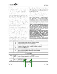
Execution Flow
Program Counter
*17~*13 *12 *11 *10 *9 *8 *7 *6 *5 *4 *3 *2 *1 *0
Mode
Initial Reset
00000
0
0
0
0
0
0
0
0
0
0
0
0
0
0
0
0
0
0
0
0
0
0
0
0
0
0
0
0
1
1
0
0
1
0
0
0
0
0
0
Timer/Event Counter 0 Overflow PF4~PF0
Timer/Event Counter 1 Overflow PF4~PF0
Skip
Program Counter+2
Loading PCL
PF4~PF0 *12 *11 *10 *9 *8 @7 @6 @5 @4 @3 @2 @1 @0
PF4~PF0 #12 #11 #10 #9 #8 #7 #6 #5 #4 #3 #2 #1 #0
PF4~PF0 S12 S11 S10 S9 S8 S7 S6 S5 S4 S3 S2 S1 S0
Jump, Call Branch
Return From Subroutine
Program Counter
Note: *12~*0: Bits of Program Counter
#12~#0: Bits of Instruction Code
@7~@0: Bits of PCL
@7~@0: Bits of PCL
S12~S0: Bits of Stack Register
PF4~PF0: Bits of Bank Register
Rev. 1.10
7
July 3, 2008
图片预览")
 HOLTEK [ HOLTEK SEMICONDUCTOR INC ]