HT36B0
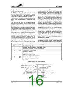
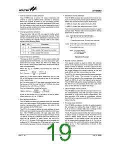
Reset
WDT Time-out
RES Reset
(Power On) (Normal Operation) (Normal Operation)
RES Reset
(HALT)
WDT Time-out
(HALT)*
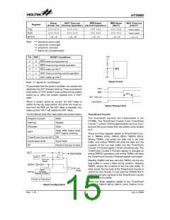
Register
TXD
1111 1111
1111 1111
---0 ---0
1111 1111
1111 1111
---0 ---0
1111 1111
1111 1111
---0 ---0
1111 1111
1111 1111
---0 ---0
uuuu uuuu
uuuu uuuu
---u ---u
RXD
INTCH
Note:
²*² stands for warm reset
²u² stands for unchanged
²x² stands for unknown
²-² stands for unimplemented
V
D
D
TO PDF
RESET Conditions
0
u
0
1
1
0
u
1
u
1
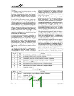
RES reset during power-up
RES reset during normal operation
RES wake-up HALT
R
E
S
WDT time-out during normal operation
WDT wake-up HALT
Reset Circuit
Note: ²u² stands for ²unchanged²
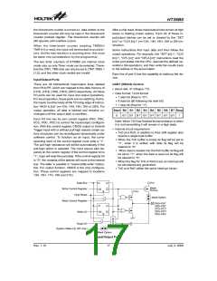
To guarantee that the system oscillator has started and
stabilized, the SST (System Start-up Timer) provides an
extra-delay of 1024 system clock pulses during system
power up or when the system awakes from a HALT
state.
V
D
D
R
E
S
t
S S T
S
S
T
T
i
m
e
-
o
u
t
When a system power-up occurs, the SST delay is
added during the reset period. But when the reset co-
mes from the RES pin, the SST delay is disabled. Any
wake-up from HALT will enable the SST delay.
C
h
i
p
R
e
s
e
t
Reset Timing Chart
The functional units chip reset status are shown below.
Timer/Event Counter
Two timer/event counters are implemented in the
HT36B0. The Timer/Event Counter 0 and Timer/Event
Counter 1 contain 16-bit programmable count-up coun-
ters and the clock comes from the system clock divided
by 4.
Program Counter
Interrupt
000H
Disable
Clear
Prescaler
Clear. After master reset,
WDT begins counting
WDT
There are three registers related to Timer/Event Coun-
ter 0; TMR0H (0CH), TMR0L (0DH), TMR0C (0EH).
Writing TMR0L only writes the data into a low byte
buffer, and writing TMR0H will write the data and the
contents of the low byte buffer into the Timer/Event
Counter 0 Preload register (16-bit) simultaneously. The
Timer/Event Counter 0 Preload register is changed by
writing TMR0H operations and writing TMR0L will keep
the Timer/Event Counter 0 Preload register unchanged.
Timer/Event Counter (0/1) Off
Input/output ports
SP
Input mode
Points to the top of stack
H
A
L
T
W
a
r
m
R
e
s
e
t
W
T
D
T
e
W
D
T
i
m
-
o
u
t
Reading TMR0H will also latch the TMR0L into the low
byte buffer to avoid a false timing problem. Reading
TMR0L returns the contents of the low byte buffer. In
other words, the low byte of the Timer/Event Counter 0
cannot be read directly. It must read the TMR0H first to
make the low byte contents of the Timer/Event Counter
0 latched into the buffer.
R
e
s
e
t
R
E
S
C
o
l
d
S
S
T
R
e
s
e
t
1
0
-
s
t
a
g
e
O
S
C
I
R
i
p
p
l
e
C
o
u
n
t
e
r
P
o
w
e
r
-
o
n
D
e
t
e
c
t
i
n
g
There are three registers related to the Timer/Event
Counter 1; TMR1H (0FH), TMR1L (10H), TMR1C (11H).
Reset Configuration
Rev. 1.10
15
July 3, 2008
图片预览")
 HOLTEK [ HOLTEK SEMICONDUCTOR INC ]