HT36B0
the timer/event counter is turned on, data written to the
timer/event counter will only be kept in the timer/event
counter preload register. The timer/event counter will
still operate until overflow occurs.
After a chip reset, these input/output lines remain at high
levels or floating (mask option). Each bit of these in-
put/output latches can be set or cleared by the ²SET
[m].i² or ²CLR [m].i² (m=12H, 14H, 16H, 18H or 20H) in-
struction.
When the timer/event counter (reading TMR0H/
TMR1H) is read, the clock will be blocked to avoid er-
rors. As this may results in a counting error, this must
be taken into consideration by the programmer.
Some instructions first input data and then follow the
output operations. For example, the ²SET [m].i², ²CLR
[m].i², ²CPL [m]² and ²CPLA [m]² instructions read the
entire port states into the CPU, execute the defined op-
erations (bit-operation), and then write the results back
to the latches or the accumulator.
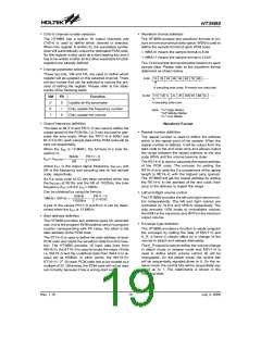
The two timer counters of HT36B0 are internal clock
mode only, so only Timer mode can be selected. There-
fore the (TM1, TM0) bits can only be set to (TM1,TM0) =
(1,0), and the other clock modes are invalid.
Each line of port A has the capability to wake-up the de-
vice.
Input/Output Ports
There are 36 bidirectional input/output lines labeled
from PA to PE, which are mapped to the data memory of
[12H], [14H], [16H], [18H], [20H] respectively. All these
I/O ports can be used for input and output operations.
For input operation, these ports are non-latching, that is,
the inputs must be ready at the T2 rising edge of instruc-
tion ²MOV A,[m]² (m=12H, 14H, 16H, 18H or 20H). For
output operation, all data is latched and remains un-
changed until the output latch is rewritten.
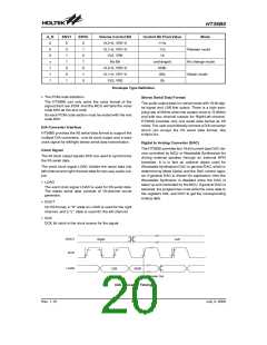
UART (RS232) Control
·
·
Baud rate: 31.25kpps± 1%
Data format: 10 bit format
¨
1 start bit (fixed to ²0²)
8 data bit (b0 following the start bit)
¨
¨
1 stop bit (fixed to ²1²)
Start B0 B1 B2 B3 B4 B5 B6 B7 Stop
0/1 0/1 0/1 0/1 0/1 0/1 0/1 0/1
0
1
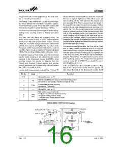
Each I/O line has its own control register (PAC, PBC,
PCC, PDC, PEC) to control the input/output configura-
tion. With this control register, CMOS output or Schmitt
Trigger input with or without pull-high resistor (mask op-
tion) structures can be reconfigured dynamically under
software control. To function as an input, the corre-
sponding latch of the control register must write a ²1².
The pull-high resistance will exhibit automatically if the
pull-high option is selected. The input source also de-
pends on the control register. If the control register bit is
²1², input will read the pad state. If the control register bit
is ²0², the contents of the latches will move to the internal
bus. The latter is possible in ²read-modify-write² instruc-
tion. For output function, CMOS is the only configura-
tion. These control registers are mapped to locations
13H, 15H, 17H, 19H and 21H).
Note: When TxD has finished its transmission or when
it is not transmitting it will remain in a high state.
·
Internal circuit requirement
¨
¨
TxD and RxD, in addition to their shift register also
require a single byte buffer
When the TxD buffer is empty its flag will be set to
²1², when it is written with data its flag will be
cleared to ²0².
¨
When data is loaded into the RxD buffer its flag will
be set to ²1², when the data is read out its flag will
be cleared to ²0².
¨
¨
When the flag for TxD or RxD is set, an interrupt will
be simultaneously generated.
TxD and RxD utilise the same interrupt vector.
V
D
D
D
a
t
a
B
u
s
D
C
Q
W
e
a
k
W
r
i
t
e
C
o
n
t
r
o
l
R
e
g
i
s
t
e
r
K
Q
P
u
l
l
-
u
p
S
V
D
D
C
h
i
p
R
e
s
e
t
M
a
s
k
O
p
t
i
o
n
R
e
a
d
C
o
n
t
r
o
l
R
e
g
i
s
t
e
r
P
A
0
0
~
~
P
P
A
B
7
7
D
C
Q
P
B
P
P
C
D
0
~
P
C
7
0
~
P
D
7
W
r
i
t
e
I
/
O
K
Q
S
P
E
0
~
P
E
3
M
U
X
R
e
a
d
o
I
/
l
O
S
y
s
t
e
m
W
a
k
e
-
U
p
(
P
A
n
y
)
M
a
s
k
O
p
t
i
o
n
Input/Output Ports
Rev. 1.10
17
July 3, 2008
图片预览")
 HOLTEK [ HOLTEK SEMICONDUCTOR INC ]