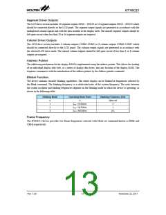
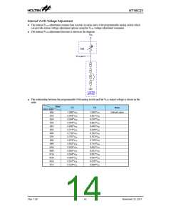
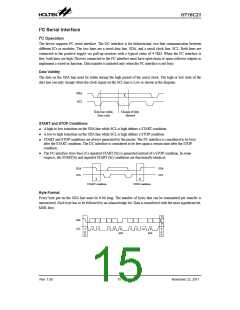
HT16C21
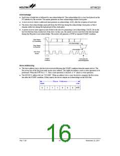
Write Operation
Byte Writes Operation
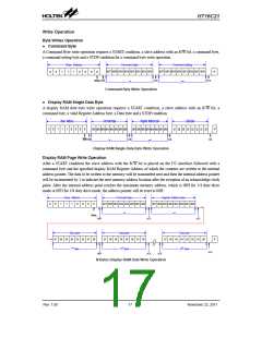
● Command Byte
A Command Byte write operation requires a START condition, a slave address with an R/W bit, a command byte,
a command setting byte and a STOP condition for a command byte write operation.
Slave Address
Command byte
Command setting
BIT7 BIT6 BIT5 BIT4 BIT3 BIT2 BIT1 BIT0
BIT7 BIT6 BIT5 BIT4 BIT3 BIT2 BIT1 BIT0
S
0
1
1
1
0
0
0
0
P
ACK
ACK
ACK
Write
1st
2nd
Command Byte Write Operation
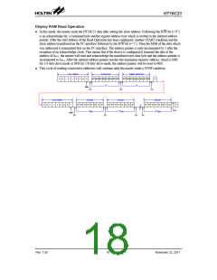
● Display RAM Single Data Byte
A display RAM data byte write operation requires a START condition, a slave address with an R/W bit, a
command byte, a valid Register Address byte, a Data byte and a STOP condition.
Slave Address
Command byte
Register Address byte
Data byte
BIT7 BIT6 BIT5 BIT4 BIT3 BIT2 BIT1 BIT0
BIT7 BIT6 BIT5 BIT4 BIT3 BIT2 BIT1 BIT0
D7
D6
D5
D4
D3
D2
D1
D0
S
0
1
1
1
0
0
0
0
P
ACK
ACK
ACK
ACK
Write
1st
2nd
Display RAM Single Data Byte Write Operation
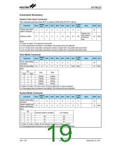
Display RAM Page Write Operation
After a START condition the slave address with the R/W bit is placed on the I2C interface followed with a
command byte and the specified display RAM Register Address of which the contents are written to the internal
address pointer. The data to be written to the memory will be transmitted next and then the internal address pointer
will be incremented by 1 to indicate the next memory address location after the reception of an acknowledge clock
pulse. After the internal address point reaches the maximum memory address, which is 09H for 1/4 duty drive
mode or 0FH for 1/8 duty drive mode, the address pointer will be reset to 00H.
Slave Address
Command byte
Register Address byte
BIT7 BIT6 BIT5 BIT4 BIT3 BIT2 BIT1 BIT0
BIT7 BIT6 BIT5 BIT4 BIT3 BIT2 BIT1 BIT0
S
0
1
1
1
0
0
0
0
1st
2nd
Write
ACK
ACK
ACK
Data byte
D4 D3
Data byte
Data byte
D7
D6
D5
D2
D1
D0
D7
D6
D5
D4
D3
D2
D1
D0
D7
D6
D5
D4
D3
D2
D1
D0
P
1st data
2nd data
Nth data
ACK
ACK
ACK
ACK
N Bytes Display RAM Data Write Operation
Rev. 1.00
17
November 22, 2011

 HOLTEK [ HOLTEK SEMICONDUCTOR INC ]