HT16C21
Internal Voltage Adjustment (IVA) Setting Command
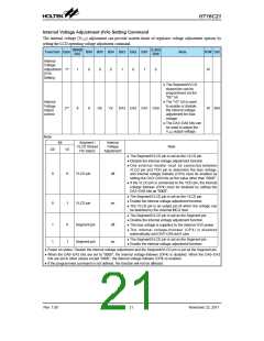
The internal voltage (VLCD) adjustment can provide sixteen kinds of regulator voltage adjustment options by
setting the LCD operating voltage adjustment command.
(MSB)
Bit7
(LSB)
Bit0
Function Byte
Bit6 Bit5 Bit4 Bit3 Bit2 Bit1
Note
R/W Def
Internal
Voltage
Adjustment 1st
(IVA)
1
0
0
0
1
0
1
0
W
Setting
● The Segment/VLCD
shared pin can be
programmed via the
“DE” bit.
Internal
Voltage
Adjust
control
● The “VE” bit is used
to enable or disable
the internal voltage
adjustment for bias
voltage.
2nd
X
X
DE
VE
DA3 DA2 DA1 DA0
W
30H
● The DA3~DA0 bits can
be used to adjust the
VLCD output voltage.
Note:
Bit
Segment /
VLCD Shared
Pin Select
Internal
Voltage
Adjustment
Note
DE
VE
● The Segment/VLCD pin is set as the VLCD pin.
● Disable the internal voltage adjustment function
● One external resister must be connected between
VLCD pin and VDD pin to determine the bias voltage,
and internal voltage follower (OP4) must be enabled by
setting the DA3~DA0 bits as the value other than “0000”.
0
0
VLCD pin
VLCD pin
off
● If the VLCD pin is connected to the VDD pin, the internal
voltage follower (OP4) must be disabled by setting the
DA3~DA0 bits as “0000”.
● The Segment/VLCD pin is set as the VLCD pin.
● Enable the internal voltage adjustment function.
0
1
on
● The VLCD pin is an output pin of which the voltage can
be detected by the external MCU host.
● The Segment/VLCD pin is set as the Segment pin.
● Disable the internal voltage adjustment function.
● The bias voltage is supplied by the internal VDD power.
1
1
0
1
Segment pin
Segment pin
off
on
● The internal voltage-follower (OP4) is disabled
automatically and DA3~DA0 don’t care.
● The Segment/VLCD pin is set as the Segment pin.
● Enable the internal voltage adjustment function.
● Power on status: Disable the internal voltage adjustment and the Segment/VLCD pin is set as the Segment pin.
● When the DA0~DA3 bits are set to “0000”, the internal voltage-follower (OP4) is disabled. When the DA0~DA3
bits are set to other values except “0000”, the internal voltage follower (OP4) is enabled.
● If the programmed command is not defined, the function will not be affected.
Rev. 1.00
21
November 22, 2011

 HOLTEK [ HOLTEK SEMICONDUCTOR INC ]