HT46R4A
Programming Considerations
register which defines the timer options and determines
how the timer is to be used. The devices can have the
timer clock configured to come from the internal clock
source. In addition, the timer clock source can also be
configured to come from an external timer pin.
Within the user program, one of the first things to con-
sider is port initialisation. After a reset, all of the I/O data
and port control registers will be set high. This means
that all I/O pins will default to an input state, the level of
which depends on the other connected circuitry and
whether pull-high options have been selected. If the port
control registers, PAC, PBC, PCC and PDC, are then
programmed to setup some pins as outputs, these out-
put pins will have an initial high output value unless the
associated port data registers, PA, PB, PC and PD, are
first programmed. Selecting which pins are inputs and
which are outputs can be achieved byte-wide by loading
the correct values into the appropriate port control regis-
ter or by programming individual bits in the port control
register using the ²SET [m].i² and ²CLR [m].i² instruc-
tions. Note that when using these bit control instruc-
tions, a read-modify-write operation takes place. The
microcontroller must first read in the data on the entire
port, modify it to the required new bit values and then re-
write this data back to the output ports.
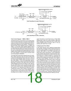
An external clock source is used when the timer is in the
event counting mode, the clock source being provided
on pin-shared pin PA4/TMR0 or PA7/TMR1. Depending
upon the condition of the T0E or T1E bit in the corre-
sponding timer control register, each high to low, or low
to high transition on the external timer input pin will in-
crement the counter by one.
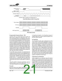
Configuring the Timer/Event Counter Input Clock
Source
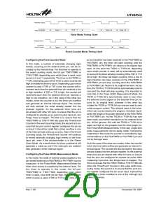
The internal timer¢s clock can originate from various
sources, depending upon which timer is chosen. The in-
ternal clock input timer source is used when the timer is
in the timer mode or in the Pulse Width Measurement
mode. Depending upon which timer is chosen this sys-
tem clock timer source may be first divided by a
prescaler, the division ratio of which is conditioned by
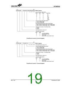
the timer control register bits PSC2~PSC0.
T
1
T
2
T
3
T
4
T
1
T
2
T
3
T
4
S
y
s
t
e
m
C
l
o
c
k
An external clock source is used when the timer is in the
event counting mode, the clock source being provided
on an external timer pin, TMR0 or TMR1 depending
upon which timer is used. Depending upon the condition
of the T0E or T1E bit, each high to low, or low to high
transition on the external timer pin will increment the
counter by one.
P
o
r
t
D
a
t
a
W
r
i
t
e
t
o
P
o
r
t
R
e
a
d
f
r
o
m
P
o
r
t
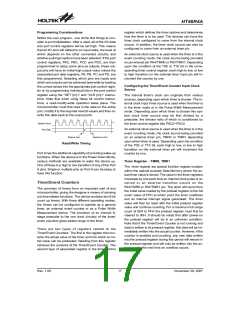
Read/Write Timing
Port A has the additional capability of providing wake-up
functions. When the device is in the Power Down Mode,
various methods are available to wake the device up.
One of these is a high to low transition of any of the Port
A pins. Single or multiple pins on Port A can be setup to
have this function.
Timer Register - TMR0, TMR1
The timer register are special function register location
within the special purpose Data Memory where the ac-
tual timer value is stored. The value in the timer registers
increases by one each time an internal clock pulse is re-
ceived or an external transition occurs on the
PA4/TMR0 or PA7/TMR1 pin. The timer will count from
the initial value loaded by the preload register to the full
count value of FFH at which point the timer overflows
and an internal interrupt signal generated. The timer
value will then be reset with the initial preload register
value and continue counting. For a maximum full range
count of 00H to FFH the preload register must first be
cleared to 00H. It should be noted that after power-on
the preload register will be in an unknown condition.
Note that if the Timer/Event Counter is not running and
data is written to its preload register, this data will be im-
mediately written into the actual counter. However, if the
counter is enabled and counting, any new data written
into the preload register during this period will remain in
the preload register and will only be written into the ac-
tual counter the next time an overflow occurs.
Timer/Event Counters
The provision of timers form an important part of any
microcontroller, giving the designer a means of carrying
out time related functions. The device contains two 8-bit
count up timers. With three different operating modes,
the timers can be configured to operate as a general
timer, an external event counter or as a Pulse Width
Measurement device. The provision of an internal 8-
stage prescaler to the one clock circuitry of the timer/
event counters gives added range to the timer.
There are two types of registers related to the
Timer/Event Counters. The first is the register that con-
tains the actual value of the timer and into which an ini-
tial value can be preloaded. Reading from this register
retrieves the contents of the Timer/Event Counter. The
second type of associated register is the timer control
Rev. 1.00
17
November 28, 2007

 HOLTEK [ HOLTEK SEMICONDUCTOR INC ]