HT46R4A
with the usual pull-high option, even if the PWM con-
figuration option has been selected.
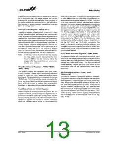
I/O Pin Structures
The following diagrams illustrate the I/O pin internal
structures. As the exact logical construction of the I/O
pin may differ from these drawings, they are supplied as
a guide only to assist with the functional understanding
of the I/O pins.
·
A/D Inputs
The device has six A/D converter inputs. All of these
analog inputs are pin-shared with I/O pins on Port B. If
these pins are to be used as A/D inputs and not as
normal I/O pins then the corresponding bits in the A/D
Converter Control Register, ADCR, must be properly
set. There are no configuration options associated
with the A/D function. If used as I/O pins, then full
pull-high resistor configuration options remain, how-
ever if used as A/D inputs then any pull-high resistor
options associated with these pins will be automati-
cally disconnected.
V
D
D
P
u
l
l
-
H
i
g
h
C
o
n
t
r
o
l
B
i
t
O
p
t
i
o
n
W
e
a
k
D
Q
P
u
l
l
-
u
p
D
a
t
a
B
u
s
W
r
i
t
e
C
o
n
t
r
o
l
R
e
g
i
s
t
e
r
C
K
Q
S
C
h
i
p
R
e
s
e
t
I
/
O
P
i
n
R
e
a
d
C
o
n
t
r
o
l
R
e
g
i
s
t
e
r
D
a
t
a
B
i
t
D
C
Q
W
r
i
t
e
D
a
t
a
R
e
g
i
s
t
e
r
K
Q
S
M
U
R
e
a
d
D
a
t
a
R
e
g
i
s
t
e
r
X
S
y
s
t
e
m
W
a
k
e
-
u
p
P
A
o
n
l
y
W
a
k
e
-
u
p
O
p
t
i
o
n
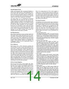
Non-pin-shared Function Input/Output Ports
V
D
D
P
u
l
l
-
H
i
g
h
C
o
n
t
r
o
l
B
i
t
O
p
t
i
o
n
W
e
a
k
D
a
t
a
B
u
s
D
Q
P
u
l
l
-
u
p
W
r
i
t
e
C
o
n
t
r
o
l
R
e
g
i
s
t
e
r
C
K
Q
S
C
h
i
p
R
e
s
e
t
P
A
4
/
T
M
R
0
P
P
A
A
5
7
/
/
I
T
N
T
R
e
a
d
C
o
n
t
r
o
l
R
e
g
i
s
t
e
r
M
R
1
D
a
t
a
B
i
t
D
C
Q
W
r
i
t
e
D
a
t
a
R
e
g
i
s
t
e
r
K
Q
S
M
U
R
e
a
d
D
a
t
a
R
e
g
i
s
t
e
r
X
I
N
T
f
o
r
P
A
5
o
n
l
y
T
M
R
0
f
o
r
P
P
A
A
4
o
n
l
y
T
M
R
1
f
o
r
7
o
n
l
y
S
y
s
t
e
m
W
a
k
e
-
u
p
W
a
k
e
-
u
p
O
p
t
i
o
n
PA4/PA5 Input/Output Ports
Rev. 1.00
15
November 28, 2007

 HOLTEK [ HOLTEK SEMICONDUCTOR INC ]