HT46R4A
In addition, on entering an interrupt sequence or execut-
ing a subroutine call, the status register will not be
pushed onto the stack automatically. If the contents of
the status registers are important and if the subroutine
can corrupt the status register, precautions must be
taken to correctly save it.
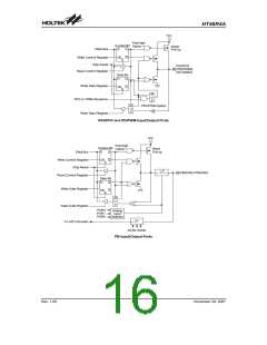
table, which are used to transfer the appropriate output
or input data on that port. With each I/O port there is an
associated control register labeled PAC, PBC, PCC and
PDC, also mapped to specific addresses with the Data
Memory. The control register specifies which pins of that
port are set as inputs and which are set as outputs. To
setup a pin as an input, the corresponding bit of the con-
trol register must be set high, for an output it must be set
low. During program initialisation, it is important to first
setup the control registers to specify which pins are out-
puts and which are inputs before reading data from or
writing data to the I/O ports. One flexible feature of these
registers is the ability to directly program single bits us-
ing the ²SET [m].i² and ²CLR [m].i² instructions. The
ability to change I/O pins from output to input and vice
versa by manipulating specific bits of the I/O control reg-
isters during normal program operation is a useful fea-
ture of these devices.
Interrupt Control Register - INTC0, INTC1
These 8-bit registers, known as INTC0 and INTC1, con-
trol the operation of both the external and internal inter-
rupts. By setting various bits within these registers using
standard bit manipulation instructions, the enable/dis-
able function of the external interrupts and each of the
internal interrupts can be independently controlled. A
master interrupt bit within these registers, the EMI bit,
acts like a global enable/disable and is used to set all of
the interrupt enable bits on or off. This bit is cleared
when an interrupt routine is entered to disable further in-
terrupt and is set by executing the RETI² instruction.
Pulse Width Modulator Registers - PWM0, PWM1
Note In situations where other interrupts may require
servicing within present interrupt service rou-
tines, the EMI bit can be manually set by the
program after the present interrupt service rou-
tine has been entered.
The device contains two Pulse Width Modulators. Each
one has its own related independent control register. For
devices with two PWM functions, their control register
names are PWM0 and PWM1. The 8-bit contents of
these registers, defines the duty cycle value for the
modulation cycle of the corresponding Pulse Width
Modulator.
Timer/Event Counter Registers - TMR0, TMR0C,
TMR1, TMR1C
The device contains two integrated 8-bit size Timer/
Event Counters. These have associated registers
known as TMR0 and TMR1, where the timer¢s values
are located. Two associated control registers, known as
TMR0C and TMR1C contain the setup information for
these two timers. Note that all timer registers can be di-
rectly written to in order to preload their contents with
fixed data to allow different time intervals to be setup.
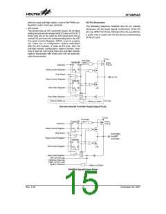
A/D Converter Registers - ADRL, ADRH,
ADCR, ACSR
The device contains a 6-channel 9-bit A/D converter.
The correct operation of the A/D requires the use of two
data registers, a control register and a clock source reg-
ister. A high byte data register known as ADRH, and a
low byte data register known as ADRL. These are the
register locations where the digital value is placed after
the completion of an analog to digital conversion cycle.
The channel selection and configuration of the A/D con-
verter is setup via the control register ADCR while the
A/D clock frequency is defined by the clock source reg-
ister, ACSR.
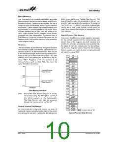
Input/Output Ports and Control Registers
Within the area of Special Function Registers, the I/O
registers and their associated control registers play a
prominent role. All I/O ports have a designated register
correspondingly labeled as PA, PB, PC and PD. These
labeled I/O registers are mapped to specific addresses
within the Data Memory as shown in the Data Memory
Rev. 1.00
13
November 28, 2007

 HOLTEK [ HOLTEK SEMICONDUCTOR INC ]