HT46R4A
Input/Output Ports
Holtek microcontrollers offer considerable flexibility on
their I/O ports. With the input or output designation of ev-
ery pin fully under user program control, pull-high op-
tions for all ports and wake-up options on certain pins,
the user is provided with an I/O structure to meet the
needs of a wide range of application possibilities.
When the corresponding bit of the control register is
written as a ²0², the I/O pin will be setup as a CMOS out-
put. If the pin is currently setup as an output, instructions
can still be used to read the output register. However, it
should be noted that the program will in fact only read
the status of the output data latch and not the actual
logic status of the output pin.
The device offers up to 27 bidirectional input/output
lines labeled with port names PA, PB, PC and PD.
These I/O ports are mapped to the Data Memory with
specific addresses as shown in the Special Purpose
Data Memory table. All of these I/O ports can be used
for input and output operations. For input operation,
these ports are non-latching, which means the inputs
must be ready at the T2 rising edge of instruction ²MOV
A,[m]², where m denotes the port address. For output
operation, all the data is latched and remains un-
changed until the output latch is rewritten.
Pin-shared Functions
The flexibility of the microcontroller range is greatly en-
hanced by the use of pins that have more than one func-
tion. Limited numbers of pins can force serious design
constraints on designers but by supplying pins with
multi-functions, many of these difficulties can be over-
come. For some pins, the chosen function of the
multi-function I/O pins is set by configuration options
while for others the function is set by application pro-
gram control.
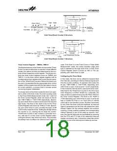
Pull-high Resistors
·
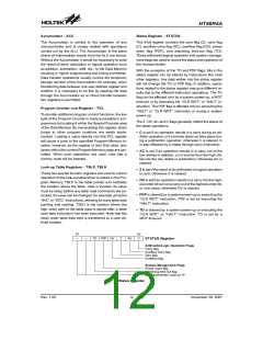
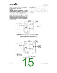
External Interrupt Input
The external interrupt pin INT is pin-shared with the
I/O pin PA5. For applications not requiring an external
interrupt input, the pin-shared external interrupt pin
can be used as a normal I/O pin, however to do this,
the external interrupt enable bits in the INTC register
must be disabled.
Many product applications require pull-high resistors for
their switch inputs usually requiring the use of an exter-
nal resistor. To eliminate the need for these external re-
sistors, all I/O pins, when configured as an input have
the capability of being connected to an internal pull-high
resistor. These pull-high resistors are selectable via
configuration options and are implemented using a
weak PMOS transistor.
·
External Timer Clock Input
The external timer pins TMR0 and TMR1 are
pin-shared with the I/O pins PA4 and PA7, respec-
tively. To configure these pins to operate as timer in-
puts, the corresponding control bits in the timer
control register must be correctly set. For applications
that do not require an external timer input, these pin
can be used as normal I/O pins. Note that if used as
normal I/O pins the timer mode control bits in the timer
control register must select the timer mode, which has
an internal clock source, to prevent the input pin from
interfering with the timer operation.
Port A Wake-up
Each device has a HALT instruction enabling the
microcontroller to enter a Power Down Mode and pre-
serve power, a feature that is important for battery and
other low-power applications. Various methods exist to
wake-up the microcontroller, one of which is to change
the logic condition on one of the Port A pins from high to
low. After a HALT instruction forces the microcontroller
into entering a Power Down condition, the device will re-
main in a low-power state until a Port A pin receives a
high to low going edge. This function is especially suit-
able for applications that can be woken up via external
switches. Note that each pin on Port A can be selected
individually to have this wake-up feature.
·
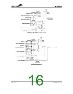
PFD Output
Each device contains a PFD function whose single
output is pin-shared with PA3. The output function of
this pin is chosen via a configuration option and re-
mains fixed after the device is programmed. Note that
the corresponding bit of the port control register,
PAC.3, must setup the pin as an output to enable the
PFD output. If the PAC port control register has setup
the pin as an input, then the pin will function as a nor-
mal logic input with the usual pull-high option, even if
the PFD configuration option has been selected.
I/O Port Control Registers
Each I/O port has its own control register PAC, PBC,
PCC and PDC, to control the input/output configuration.
With this control register, each CMOS output or input
with or without pull-high resistor structures can be re-
configured dynamically under software control. Each pin
of the I/O ports is directly mapped to a bit in its associ-
ated port control register. For the I/O pin to function as
an input, the corresponding bit of the control register
must be written as a ²1². This will then allow the logic
state of the input pin to be directly read by instructions.
·
PWM Outputs
The devices contain two PWM outputs PWM0 and
PWM1 are pin shared with pins PD0 and PD1,
respectively. The PWM output functions are chosen
via configuration options and remain fixed after the
device is programmed. Note that the corresponding
bit or bits of the port control register, PDC, must setup
the pin as an output to enable the PWM output. If the
PDC port control register has setup the pin as an in-
put, then the pin will function as a normal logic input
Rev. 1.00
14
November 28, 2007

 HOLTEK [ HOLTEK SEMICONDUCTOR INC ]